
Submitted:
09 December 2025
Posted:
11 December 2025
You are already at the latest version
Abstract
This paper presents the design and implementation of a 64-Multi-Phased Time-to-Digital Converter (TDC64) architecture on a low-cost Cyclone V FPGA. Operating at 500 MHz, the architecture successfully achieves a theoretical resolution of 31.25 picoseconds (ps). The modular design leverages a multi-phased counter methodology to significantly enhance temporal granularity. The performance was comprehensively characterized in two stages. Internal analysis, using the Signal Tap Logic Analyzer, confirmed the design's integrity, yielding a measurement result of 9660 for a 300 ns interval, representing a low deviation of approximate 0.62 %. Linearity tests conducted over a 20 ns span showed excellent performance with differential nonlinearity (DNL) ranging from +0.053 to -0.101 and integral nonlinearity (INL) between -0.192 and -0.218. External testing, utilizing a waveform generator and oscilloscope, revealed an uncompensated resolution of 47.43 ps (34 % deviation). Mitigating the noise, the compensated resolution for an interval of 300 ns result in 9,596, a resolution of 31.263 picoseconds, which represents 0.04%. A remarkable result close to the theoretically expected value. The mean values were employed to evaluate the linearity, yielding DNL of +0,0560 and -0,0129, as well as INL of +0,0484 and -0,2104. Representing high linearity and high resolution compared with a previous noisy entry signal. This work demonstrates that high-end timing performance is attainable on cost-effective FPGA platforms.
Keywords:
multi-phased clock
; time to digital converter
; HDL language
; FPGA
; cyclone V
I. Introduction
Time-to-Digital Converters (TDCs) are a fundamental component in modern instrumentation, with an evolutionary history tracing back to the 1970s [1]. The primary driver of their continuous development is the relentless pursuit of sub-nanosecond precision in event measurement, representing a critical and persistent challenge for the scientific community [2]. Recent technological advances have substantially transformed these components, allowing for the implementation of increasingly complex, high-resolution designs on accessible platforms [3]. Consequently, the confluence of improved measurement precision and the substantial potential for cost reduction inherent in modern Time-to-Digital Converter (TDC) implementations drastically broadens their operational scope [4]. The achievement of sub-nanosecond resolution, often utilizing accessible platforms such as Field-Programmable Gate Arrays (FPGAs), translates directly into the ability to perform high-fidelity temporal analysis across diverse scientific and engineering disciplines [5]. This dual benefit, i.e. high performance attained economically, is the primary enabler for integrating TDCs into previously prohibitive or restricted application areas, fundamentally transforming areas like high-throughput data acquisition, critical industrial sensing, and advanced medical imaging systems [6].
The realization of Time-to-Digital Converters (TDCs) exhibits substantial technological versatility, enabling their implementation across diverse hardware platforms, specifically in both specialized Application-Specific Integrated Circuits (ASICs) and highly reconfigurable Field-Programmable Gate Arrays (FPGAs) [7]. This wide-ranging deployability underscores the critical role of TDCs in numerous advanced scientific and industrial domains. Their utility is particularly pronounced in precision timing applications, such as high-speed synchronization systems, prominently featuring in all-digital phase-locked loops (ADPLLs) [8].
Furthermore, TDCs are essential components for real-time sensing and accurate distance measurement methodologies, encompassing time-of-flight (ToF) systems and sophisticated light detection and ranging (LiDAR) techniques [9]. They are also indispensable in high-resolution imaging systems, most notably in positron emission tomography (PET) and advanced fluorescence lifetime imaging microscopy [10]. Beyond these specialized fields, TDCs prove instrumental in general-purpose instrumentation, such as digital storage oscilloscopes, and for critical integrated circuit monitoring, exemplified by their use in on-chip temperature sensors [11].
Fundamentally, the efficacy and performance of any Time-to-Digital Converter architecture are strictly governed by three critical performance metrics: resolution, range, and linearity [12]. These parameters dictate the minimum detectable time, the maximum measurable span, and the accuracy of the conversion across the range, respectively [13]. Among the established methodologies, the counter-based approach is widely acknowledged as the simplest and most inherently reliable technique for direct time measurement, exhibiting high precision when operating synchronously [14]. Nonetheless, this direct counter-based conversion method inherently encounters a significant and fundamental limitation: the measured time interval (TIM), delimited by the arrival of the Start and Stop input pulses, frequently exhibits an asynchronous relationship with the rising or falling edges of the continuous, periodic reference clock signal [15]. This lack of inherent synchronization is the primary challenge, as the temporal alignment of the events being measured is statistically independent of the clock period, rendering a direct, precise mapping of the fractional time interval highly problematic for high-resolution applications [16].
This lack of synchronization intrinsically introduces quantization errors. Specifically, these errors stem from the residual temporal discrepancies, denoted as Δ_Start and Δ_Stop, between the rising edges of the start and stop input pulses and the nearest active edge of the system clock [17]. This unavoidable challenge, which limits the achievable precision, is conceptually depicted in Figure 1, illustrating the basic structural components of a direct measure counter TDC.
Figure 1 conceptually outlines the operation of a conventional counter-based TDC. The time to be measured (TM) is delimited by Pulse 1 (Start) and Pulse 2 (Stop). This Time Measured signal (TM) simultaneously acts as the Enable for the digital Counter. The counter increases its output (Dout) with each edge of the Clock signal while enabled. The total measured time is the sum of the full clock cycles counted, plus the fractional time intervals ΔStart and ΔStop. As the counter registers only the integer number of clock cycles between the start and stop events, the residual time represented by ΔStart and ΔStop is discarded, thus limiting the resolution to the period of the clock (Tclock).
To overcome the quantization limitations inherent to single-clock counter architectures, the multi-phase counter method is employed to significantly enhance resolution [18]. This technique involves applying multiple, phase-shifted versions of the reference clock to a set of independent counters, whose individual outputs are then summed to yield the final measurement. This approach effectively subdivides the fundamental clock period, thereby achieving finer temporal granularity [19]. Figure 2 provides a visual representation of this method, which forms the core architectural principle implemented in this study.
As detailed in Figure 2, the multi-phase counting process utilizes the Time Measured (TM) signal to enable four independent counters, each clocked by a phase-shifted version of the clock (clk_0, clk_90, clk_180, and clk_270). The rising edges of these phase clocks are detected within the active TM window. By summing the accumulated counts from all channels, the system effectively registers more events over the same time span than a single counter, leading to a measured output (Dout) that is four times more precise than the base clock period. This concurrent counting mechanism achieves a substantial reduction in the minimum detectable time interval, directly increasing the TDC's resolution [20]. Formally, the theoretical limit of resolution in a multi-phase counter architecture is inversely proportional to the number of phases utilized [21]. The theoretical resolution (TResolution) is determined by dividing the period of the base clock (Tclock) by the total number of phases (Nnumber of phases), as defined by Equation (1).
TResolution = Tclock / Nnumber of phases
Building upon this principle, this paper formally introduces the design and implementation of a 64-Multi-Phased Time-to-Digital Converter architecture achieved on a low-cost Cyclone V FPGA. This approach successfully utilizes the 64 phase-shifted clocks at 500 MHz, succeeding the theoretical resolution of 31.25 ps. The modularity and portability of the design are ensured, as all circuits are described using a generic Hardware Description Language (HDL), specifically System Verilog and Verilog, allowing for broader compatibility and future scaling. The following sections detail the architecture, characterize the performance, and compare these results against established literature.
II. Architecture, Design, and Simulation
This section thoroughly delineates the architectural foundation, modular design, and functional verification of the 64-Multi-Phased Time-to-Digital Converter (TDC64). The discussion begins with a detailed block-level breakdown of the system, emphasizing the rationale behind the selection and implementation of the seven key modules designed using generic Hardware Description Language (HDL) for optimal portability and resource efficiency. Subsequently, the system's performance is evaluated through simulation, focusing on the constrained timing environment and confirming the theoretical resolution achieved within the low-cost Field-Programmable Gate Array (FPGA).
A. Architecture and Design
The TDC64 was intentionally engineered using a highly modular and portable design methodology, utilizing generic System Verilog and Verilog HDL. This approach ensures maximal compatibility and intrinsic scalability across diverse technological platforms, a critical consideration for future adaptability. The complete TDC architecture is structured around seven distinct functional blocks, three of which are designed with inherent scalability to precisely manage an increased number of phases, a design choice fundamental to the resolution enhancement.
The measurement process begins with the Delta Time (DT) block, which utilizes an XOR logic gate to precisely determine the time interval between the two asynchronous input signals (Pulse A and Pulse B). The logical output of the DT block is the Time Measured (TM) signal, which acts as the crucial Enable signal for the subsequent Counter Set (CS) block. The system’s foundational timing is governed by the Clock Generator (CG) block, which is accomplished as a 500 MHz gated ring oscillator (GRO). This choice of a GRO minimizes logic utilization while concurrently maximizing operational performance. The CG block comprises three D-latches, featuring an asynchronous low-reset and a high-enable signal. The ring is closed via a delay chain that incorporates a single inverter, introducing a calibrated 1000 picosecond delay. The feedback connection, where the register output links to the inverter input and the inverter output links to the data input of the next register, establishes the precise mechanism for stable 500 MHz oscillation.
The core innovation of the design resides in the Multi-Phased Clock (MPC) block, which is tasked with generating the precise 64-phase clock tree. CLK0 serves as the primary clock at 500 MHz. The full set of 64 signals is achieved by generating CLK32 through a simple inversion of CLK0, and by delaying the remaining 62 clocks using carefully tuned buffers. By dividing the 180° phase shift (half the clock period) into 32 equal segments, the design achieves a uniform and incremental phase step of 5.625° between adjacent clocks. At the operating frequency of 500 MHz, this phase step corresponds to a time difference of exactly 31.25 picoseconds (ps), a value that establishes the theoretical limit of the TDC's resolution.
The resulting multi-phase clocks feed the Counter Set (CS) block, which consists of 64 independent 8 bit counters. Each counter is individually clocked by one of the 64 delayed clock signals and is activated concurrently by the TM signal output from the DT block. The accumulated counts from all channels are then aggregated by the Adder Counter (AC) block, which computes the cumulative sum of all 64 CS block outputs. This final summation directly determines the measured time and, consequently, defines the system's effective resolution. Finally, the Single Pulse (SP) block generates a momentary pulse following Pulse B, marking the precise completion of the measurement interval. This terminal pulse subsequently triggers the Dlatch Vector (DV) block, enabling the reliable capture and storage of the final measurement result into external memory. The comprehensive architectural relationship of the TDC64 blocks is schematically represented in Figure 3.
Figure 3 visually represents the Block Diagram of the 64 Multi-Phased 500 MHz Clocks (TDC64), which is the integration of the seven functional blocks, as described earlier. This comprehensive architecture, designed in HDL, requires rigorous functional verification, therefore, the following section, Simulation, details the methodology and results confirming the design's expected theoretical performance.
B. Simulation
The theoretically derived performance metrics of the 64-Multi-Phased Time-to-Digital Converter (TDC64) architecture necessitated a phase of rigorous functional simulation to confirm the integrity of the design implementation. This crucial verification step was executed within the industry-standard environment provided by the ModelSim Intel FPGA Starter Edition 2020.1 software, which is widely recognized for its robust capabilities in digital design analysis and waveform inspection.
To optimize the simulation run-time and enhance the clarity of the resulting waveforms, a simplification was applied to the Clock Generator (CG) block. Specifically, the CG block's enabled input, which conventionally manages system startup via reset and enable signals, was fixed at a constantly high logic level. This tactical decision effectively minimized the number of interacting control signals during the core measurement phase. Fundamentally, the precise control over all system frequencies and the rigorous timing requirements of the high-resolution architecture were accurately managed and defined using a dedicated Synopsys Design Constraints (SDC) file. This critical constraint step ensured that the design specifications strictly adhered to the challenging 500 MHz operating frequency, thereby maintaining the integrity of the intended high-resolution temporal partitioning.
For ensuring methodological consistency throughout the entire validation process, the specific time interval being measured, i.e. the duration between the asynchronous input signals, Pulse A and Pulse B, was uniformly calibrated to 300 nanoseconds (ns) across all simulation trials. This fixed 300 ns interval was carefully selected to precisely match the target delay employed in both the subsequent internal (Signal Tap) and external experimental characterization stages. This congruence facilitates a direct and robust comparison between the simulated outcomes and the empirically measured results. The resultant outcome of the simulation analysis is visually presented in Figure 4. Due to the inherent complexity and the high multiplicity of signal channels (64 phase clocks and 64 counters) within the design, a set of 48 intermediate output signals was intentionally omitted from the visual representation in Figure 4. This careful selection was implemented solely to enhance the scannability and analytical clarity of the displayed waveforms.
The visual outcome presented in Figure 4 selectively illustrates the temporal waveforms critical for functional confirmation. Specifically, the display captures the state of the initial four phase clocks CLK0 to CLK3 and the final four clocks CLK60 to CLK63 from the 64-phase clock tree, alongside eight representative intermediate signals (C280 to C350), which represent a partial accumulation of the aggregated counts.
Fundamentally, the results derived from the functional simulation exhibit precise alignment with the expected theoretical value for the calibrated 300 ns measurement interval. The total accumulated sum recorded by the system was 9600. This count is mathematically consistent with the number of clock edges expected for a 300 ns period divided by the theoretical resolution of 31.25 ps (i.e., 300 ns / 31.25 ps = 9600). This congruence unequivocally confirms the design's achievement of its target resolution of 31.25 ps.
The successful congruence between the simulated result (9600) and the calculated theoretical count definitively validates the design's fundamental functional integrity. Nevertheless, to ensure the robustness and applicability of this high-resolution architecture, its true performance capabilities, especially when subjected to non-ideal physical constraints and signal noise inherent in an operational system, must be empirically characterized and confirmed within a real-world operating environment. This critical empirical validation forms the precise focus of the subsequent section.
III. Environment and Results
This section outlines environmental tests conducted initially using internal stimuli via the Signal Tap Logic Analyzer, followed by external signals applied to the input of the TDC64 to measure a specific interval. Additionally, it includes a discussion of experimental results that compares matching improvements and provide an evaluation against similar studies.
A. Environment Testing
The system is comprised of a bench integrating a DE10-Nano development board alongside a personal computer. The PC is configured with Intel's Quartus Prime Lite 20.1.1 Electronic Design Automation software. The FPGA used belongs to the Cyclone V family, specifically the 5CSEBA6U23I7 device. Current logic utilization is minimal, accounting for only 1% of the available resources at 528 registers and 6% of the total pins.
Internal evaluations were performed utilizing the Signal Tap Logic Analyzer, an embedded signal analysis and debugging utility integrated in Quartus Prime. By operating on actual hardware, Signal Tap enables the capture of logic signal waveforms from the design, allowing for the estimation of certain outcomes based on this tool's output.
The setup comprises a DSO-X3024T oscilloscope and a 33600A Series waveform generator. Initially, the generator was configured to output two square waves at a frequency of 10 kHz, each delayed by 300 nanoseconds and with an amplitude of 3.3 Vpp. These signals functioned as the external input for the TDC64. Subsequently, the signal was modified to a pulse with a slew rate of 40 ns and maintained at 3.3 Vpp at the same frequency. The environment also includes a set of male/female jumper wires for accessing the 40-pin GPIO header, as well as BNC cables featuring various shielding levels for both signal and ground, and resistors for 50-ohm impedance matching.
B. Experimental Results
The experimental results were evaluated in two phases: initially by analyzing internal FPGA signals using generated signals within the device, and subsequently by assessing external signals with waveform equipment and an oscilloscope. To evaluate the internal signals of the design, a 300-nanosecond interval was established in Signal Tap, facilitating verification of the TDC64’s functionality. This methodology enabled comprehensive analysis of the FPGA's internal signals and systematic assessment of system behavior.
Figure 5 illustrates the same time interval selected for the simulation, with the measured result being 9660. This represents a deviation of approximately 0.62%, remaining within the 1% margin.
Linearity assessments were performed using 64 samples over 21-time intervals, ranging from 290 ns to 310 ns in 1 ns increment. Since 64 samples remain constant for any specific interval, the differential nonlinearity (DNL) values varied between +0.053 and -0.101, while the integral nonlinearity (INL) values ranged from -0.192 to -0.218. Figure 6 presents the differential nonlinearity (a) and integral nonlinearity (b) as observed in Signal Tap.
To address significant noise issues, Signal B was reassigned to an alternative GPIO pin expansion header, resulting in a substantial reduction in interference.
External signals were connected to GPIO pins Signal A and Signal B, which were originally assigned to adjacent positions in the pin planner. However, significant signal reflections and crosstalk adversely impacted the accuracy of TDC measurements, resulting in inconsistencies when compared to both simulation data and Signal Tap observations.
Figure 7 illustrates the external signal produced by the waveform generator and recorded using an oscilloscope. Although enhancements have been implemented, under-overshoot can still be detected on both signals: Signal A (blue) at 36 ns and Signal B (red) at 34 ns.
The FPGA's Hard Processor System (HPS) was configured to execute custom algorithms, facilitating enhanced system flexibility and adaptability under varying operating conditions. This configuration enabled the accurate measurement of a 300-nanosecond external interval over 1450 samples. Sequential measurements of the two signals were performed every 100 microseconds, aligning with the 10 kHz period of each signal. Data collected from these measurements were compiled into an .csv file containing 1450 entries, which produced an average value of 6325.
By dividing the 300-nanosecond measurement interval by 6,325, a resolution of 47.43 picoseconds was achieved, representing a 34% deviation from the theoretical value, considered a high deviation. The average value was employed to evaluate system linearity, yielding differential nonlinearity (DNL) values of +0.0572 and -0.0284, as well as integral nonlinearity (INL) values of +0.1237 and -0.6215. Representing a good linearity.
Noise mitigation techniques were implemented, including replacing standard oscilloscope cables with BNC cables featuring a more effective shielding mesh rated at 50 ohms. Series resistors were added to the GPIO input for improved impedance matching. Furthermore, square wave signals were replaced by equivalent pulses with a 40ns slew rate, as direct entry of signals A and B into the gate caused reflections due to abrupt transitions in square waves.
These actions led to a significant improvement in the entry signals. Figure 8 illustrates the data extracted from the oscilloscope’s input signal after mitigating noises.
The data obtained from measurements conducted without overshooting were recorded in a second .csv file, and the corresponding analysis results are presented below.
As with the previous data set, 1,450 samples were extracted, yielding a mean value of approximately 9,596 and a resolution of 31.263 picoseconds, which represents 0.04%. This result is remarkably close to the theoretically expected value. The mean values were employed to evaluate again the linearity, yielding DNL values of +0.0560 and -0.0129, as well as INL values of +0.0484 and -0.2104. Representing better linearity compared with the noisy entry signal.
Figure 9 presents the differential nonlinearity (a) and integral nonlinearity (b) calculated from the external signal after noise mitigation.
A comparison between samples exhibiting overshoots and those without reveals that, in the absence of noise, the mean closely approximated the theoretical value. Additionally, these samples demonstrated a lower standard deviation relative to their noisy counterparts. Table I provides descriptive statistics summarizing the entire sample set.

Table I.
Descriptive Statistics.
| Samples | Overshoot | Mean | Standard Deviation |
| 1450 | With | 6325.14 | 78.77 |
| 1450 | Without | 9596.29 | 43.54 |
The comparative analysis clearly demonstrates that noise mitigation techniques substantially enhance both the accuracy and linearity of the measurement system. The results indicate that the mean value for noise-free samples is not only closer to the theoretical expectation but also exhibits a significantly reduced standard deviation, highlighting improved consistency across measurements. This improvement underscores the critical role of effective signal conditioning in high-precision timing applications.
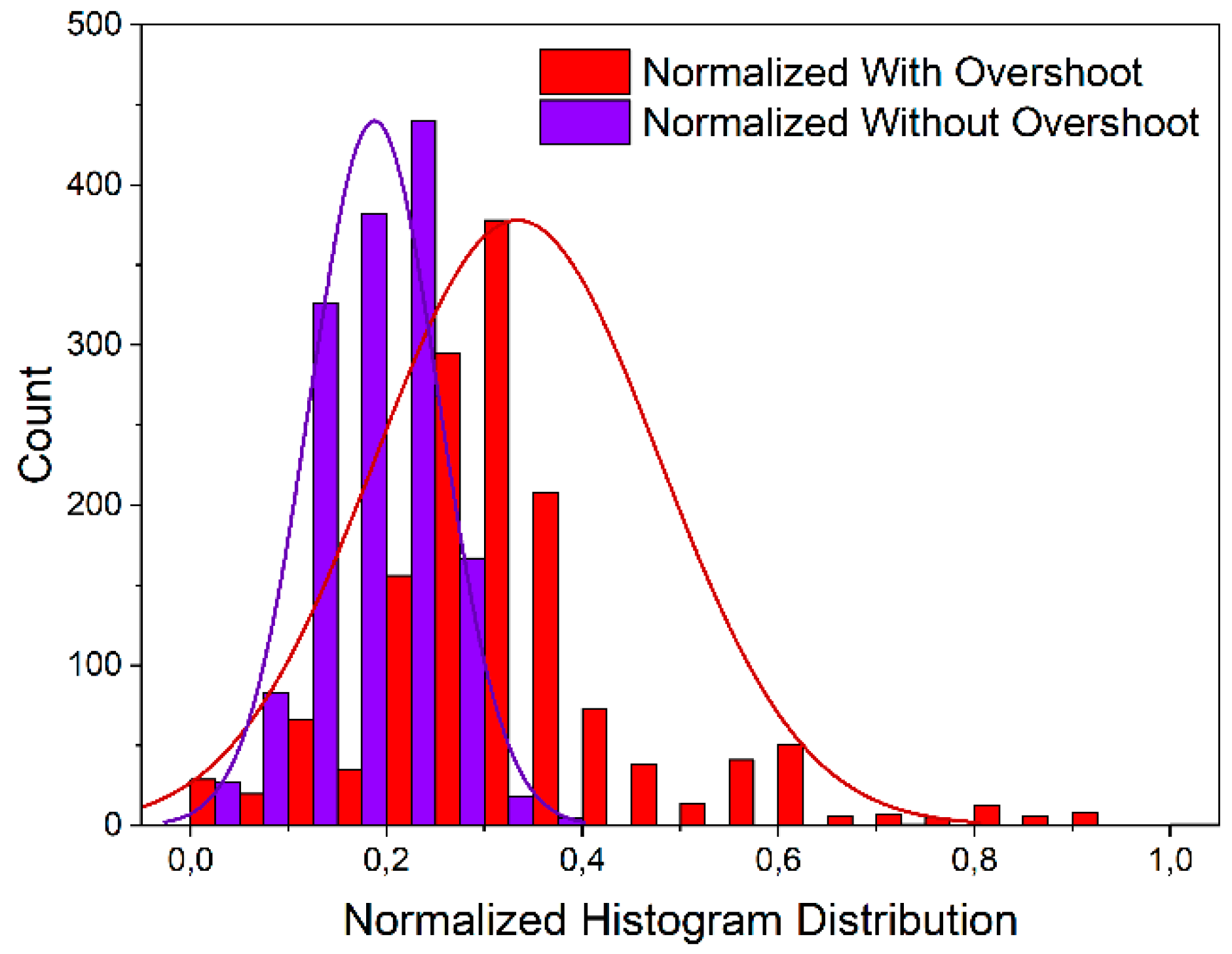
Figure 10 illustrates a comparative histogram of two normalized distributions: one incorporating overshoot (red) and one without overshoot (blue). The x-axis represents the normalized histogram distribution ranging from 0.0 to 1.0, while the y-axis indicates the count of occurrences within each bin, extending up to 500.
The distribution with overshoot exhibits a broader spread across the entire range, with a peak centered around 0.35. This suggests a higher range of midrange values and increased variability. In contrast, the distribution without overshoot is more concentrated in the lower range, peaking near 0.2, and tapering off rapidly beyond 0.4, indicating a more compact and less dispersed dataset.
Both histograms are overlaid with smooth density curves that highlight the underlying probability distributions. The red curve (with overshoot) is flatter and wider, reflecting greater dispersion, while the blue curve (without overshoot) is narrower and taller, emphasizing the concentration of values in the lower range.
This comparison illustrates the impact of overshoot on measurements, where the presence of overshoot leads to a spread distribution across the normalized scale, whereas its absence results in clustering toward expected values.
C. Discussions and Considerations
All TDC64 counters are activated by the XOR logic gate signal output from the DT block. Due to the significant under-overshoot observed, the counters might have been momentarily disabled from counting during this period. Not considering the under-overshoot, the resolution varied by 34%, resulting in a resolution of 47.43 picoseconds. Given that signal A exhibited an under-overshoot of 36 ns and signal B of 34 ns, and assuming the counters remained inactive during this time, the effective time interval can be approximated as 230 nanoseconds. Recalculating the resolution with this interval is obtained by a resolution of 36.36 picoseconds.
Eliminating the overshooting the high resolution and the high linear approach of the multi-phased TDC64 was confirmed, allowing a meaningful comparison with previous studies specifically referenced in [22], comparing analysis of this work with earlier techniques. In both internal and external approaches, the TDC64 proved to be precise and quite linear.
FPGA vendors such as Altera and Xilinx offer families tailored for both high-end and low-end applications. While the Stratix series from Altera and the Virtex series from Xilinx cater to high-end designs, the Cyclone series from Altera, along with the Kintex7 and Spartan series from Xilinx, are optimized for low-cost applications.
The FPGA most closely related to this work is the Kintex7 [23] (Wang et al., 2016), which utilizes three phase-locked loops (PLLs) within its clock management block to produce eight-phase clock signals. The initial PLL converts a 200 MHz input clock into a 700 MHz output, while the remaining two PLLs generate eight outputs at an identical frequency, each with a 22.5-degree phase offset. Flip-flops are configured to be triggered on alternating clock edges. Two principal methods are used to generate multiphase clocks: introducing phase shifts via a delay line or employing PLLs/DLLs.
A gated ring oscillator (GRO) is utilized to generate the primary clock in this work, which is subsequently phase-shifted to construct the clock tree with a phase increment of 5.625 degrees.
This approach efficiently reduces the number of blocks, resulting in lower logic utilization while preserving both performance and portability, all without relying on proprietary instructions. Achieving a resolution around 31.26 picoseconds demonstrates the capability of low-cost FPGA solutions.
This work presents a comparative summary of three FPGA-based Time-to-Digital Converter (TDC) implementations: Wang et al. [23], Mattada et al. [22], and the proposed architecture described herein. The evaluation encompasses essential performance metrics, including number of phases, operating frequency, time resolution, linearity characteristics, and the specific FPGA platform utilized.
The proposed design in This Work demonstrates significant improvements across multiple phases. It utilizes 64 phases, doubling the phase count of Mattada et al. and quadrupling that of Wang et al., thereby enhancing temporal granularity. Despite operating at the same frequency as Mattada et al. (500 MHz), it achieves a superior time resolution of 31.26 ps, which is nearly half that of Mattada et al. (62.5 ps) and substantially better than Wang et al. (89.9 ps).
In terms of linearity, the proposed design exhibits markedly reduced Differential Non-Linearity (DNL) and Integral Non-Linearity (INL). The DNL ranges from +0.06 to -0.13, and the INL from +0.05 to -0.21, indicating high precision and minimal deviation. These values are significantly lower than those reported by Wang et al. and Mattada et al., whose DNL and INL values exceed ±0.8 in some cases.
Furthermore, the implementation leverages the Cyclone 5 FPGA platform (low cost in 2025), which reflects an update in terms of design becoming potentially more efficient hardware environment compared to the Kintex7 (2016) and Virtex 5 (2022) platforms used in prior works.
Overall, the proposed architecture achieves enhanced resolution and linearity without increasing the operating frequency, showcasing an efficient and scalable approach to high-precision TDC design on cost-effective FPGA platforms.
IV. Conclusions
This work shows that high-end performance is attainable with a low-cost FPGA. The modular design of the TDC64 enables scalability, allowing for an increased number of phases to enhance resolution while preserving linearity. By adjusting the number of phases within the MPC, CS, and AC blocks and fine-tuning the corresponding delay times for the target frequency, the desired phase variation can be effectively achieved. This modular adaptability ensures flexibility in optimizing resolution while maintaining system stability and performance.
The circuits were implemented using a generic and portable HDL language, with the frequency multi-phased sixty-two times at 5.625-degree, achieving a theoretical resolution of 31.25 picoseconds in internal approach with Signal Tap Logic Analyzer.
The HPS programming of the FPGA enables comprehensive statistical analysis of over 1,450 samples, delivering enhanced insights into the system's performance.
An inadequately prepared external environment resulted in undershooting and overshoot in the generated signals, highlighting the necessity for enhanced impedance matching between cables and equipment to reduce these phenomena.
Noise mitigation techniques were implemented and these actions led to a significant improvement in the entry signals. Yielding a resolution of 31.263 picoseconds, which represents 0.04% of the expected value.
These results demonstrate that the TDC64 design not only delivers a substantial leap in temporal resolution but also maintains superior linearity compared to previous approaches. The combination of scalability, cost-effectiveness, and robust statistical validation positions this architecture as a strong candidate for applications demanding high precision and reliability.
Importantly, the successful integration of noise mitigation and impedance matching further validates the system’s practical viability for deployment in real-world measurement environments.
These promising results underscore significant progress in the development of multi-phased TDC for high-resolution applications in FPGA Cyclone V, offering improvements over prior techniques.
Acknowledgements
The authors express their acknowledgement to their respective institutions and the National Council for Scientific and Technological Development (CNPq) under the CPSAE Project (Grant No. 422360/2023-6) for supporting this work.
References
- M. P. Mattada and H. Guhilot, “Time-to-digital converters—A comprehensive review,” International Journal of Circuit Theory and Applications, vol. 49, no. 3, pp. 778–800, Mar. 2021. [CrossRef]
- S. Tancock, E. Arabul, and N. Dahnoun, “A Review of New Time-to-Digital Conversion Techniques,” IEEE Transactions on Instrumentation and Measurement, vol. 68, no. 10, pp. 3406–3417, Oct. 2019. [CrossRef]
- H. Xia, X. Yu, J. Zhang, and G. Cao, “A Review of Advancements and Trends in Time-to-Digital Converters Based on FPGA,” IEEE Transactions on Instrumentation and Measurement, vol. 73, pp. 1–25, 2024. [CrossRef]
- SCOTT TANCOCK, “The Efficient Design of Time-to-Digital Converters,” Dec. 2021.
- F. Pfeifle, “Real-Time Signal Processing on Field Programmable Gate Array Hardware,” 2018, pp. 385–417. [CrossRef]
- T. Moeinfard, E. Ghafar-Zadeh, and S. Magierowski, “CMOS Point-of-Care Diagnostics Technologies: Recent Advances and Future Prospects,” Micromachines, vol. 15, no. 11, p. 1320, Oct. 2024. [CrossRef]
- R. Machado, J. Cabral, and F. S. Alves, “Recent Developments and Challenges in FPGA-Based Time-to-Digital Converters,” IEEE Transactions on Instrumentation and Measurement, vol. 68, no. 11, pp. 4205–4221, Nov. 2019. [CrossRef]
- E. B. Priyanka, S. Thangavel, and V. G. Pratheep, “Enhanced Digital Synthesized Phase Locked Loop with High Frequency Compensation and Clock Generation,” Sensing and Imaging, vol. 21, no. 1, p. 43, Dec. 2020. [CrossRef]
- Ronchini Ximenes, P. Padmanabhan, and E. Charbon, “Mutually Coupled Time-to-Digital Converters (TDCs) for Direct Time-of-Flight (dTOF) Image Sensors ‡,” Sensors, vol. 18, no. 10, p. 3413, Oct. 2018. [CrossRef]
- J. J. Vaquero and P. Kinahan, “Positron Emission Tomography: Current Challenges and Opportunities for Technological Advances in Clinical and Preclinical Imaging Systems,” Annual Review of Biomedical Engineering, vol. 17, no. 1, pp. 385–414, Dec. 2015. [CrossRef]
- N. Corna, F. Garzetti, N. Lusardi, and A. Geraci, “Digital Instrument for Time Measurements: Small, Portable, High–Performance, Fully Programmable,” IEEE Access, vol. 9, pp. 123964–123976, 2021. [CrossRef]
- Z. Cheng, X. Zheng, M. J. Deen, and H. Peng, “Recent Developments and Design Challenges of High-Performance Ring Oscillator CMOS Time-to-Digital Converters,” IEEE Transactions on Electron Devices, vol. 63, no. 1, pp. 235–251, Jan. 2016. [CrossRef]
- S. Henzler, “Time-to-Digital Converter Basics,” 2010, pp. 5–18. [CrossRef]
- J. Raman, T. Cromheecke, S. Ooghe, B. Saux, and P. Rombouts, “A Double-Edge Triggered Asynchronous Gray Counter for Use as a Coarse Counter in VCO ADCs,” IEEE Transactions on Circuits and Systems II: Express Briefs, vol. 71, no. 9, pp. 4121–4125, Sep. 2024. [CrossRef]
- Y. Li, F. Gu, G. Harris, A. Ball, N. Bennett, and K. Travis, “The measurement of instantaneous angular speed,” Mechanical Systems and Signal Processing, vol. 19, no. 4, pp. 786–805, Jul. 2005. [CrossRef]
- D. Mulvin, “The media of high-resolution time: Temporal frequencies as infrastructural resources,” The Information Society, vol. 33, no. 5, pp. 282–290, Oct. 2017. [CrossRef]
- T. Zhou, Z. Zuo, and Y. Wang, “Quantizer-Based Triggered Control for Chaotic Synchronization With Information Constraints,” IEEE Transactions on Cybernetics, vol. 48, no. 8, pp. 2500–2508, Aug. 2018. [CrossRef]
- N. Lusardi, F. Garzetti, A. Costa, E. Ronconi, and A. Geraci, “From Multiphase to Novel Single-Phase Multichannel Shift-Clock Fast Counter Time-to-Digital Converter,” IEEE Transactions on Industrial Electronics, vol. 71, no. 8, pp. 9886–9894, Aug. 2024. [CrossRef]
- X. Wang et al., “CLOCK: Online Temporal Hierarchical Framework for Multi-scale Multi-granularity Forecasting of User Impression,” in Proceedings of the 32nd ACM International Conference on Information and Knowledge Management, New York, NY, USA: ACM, Oct. 2023, pp. 2544–2553. [CrossRef]
- F. Villa et al., “SPADs and TDCs for photon-counting, timing and gated-imaging at 30 ps resolution and 60% efficiency,” in 2018 IEEE Nuclear Science Symposium and Medical Imaging Conference Proceedings (NSS/MIC), IEEE, Nov. 2018, pp. 1–5. [CrossRef]
- N. Lusardi, S. Salgaro, F. Garzetti, N. Corna, G. Ticozzi, and A. Geraci, “FPGA-based Multi-Phase Shift-Clock Fast-Counter Time-to-Digital Converter for Extremely-Large Number of Channels,” in 2020 IEEE Nuclear Science Symposium and Medical Imaging Conference (NSS/MIC), IEEE, Oct. 2020, pp. 1–4. [CrossRef]
- Mahantesh Mattada, Hansraj Guhilot “62.5 ps LSB resolution multi-phase clock Time to Digital Converter (TDC) implemented on FPGA” Journal of King Saud University - Engineering Sciences 34 (2022) 418-424 . [CrossRef]
- Wang, Y., Kuang, P., Liu, C., 2016. “A 256-channel multi-phase clock sampling-based time-to-digital converter implemented in a Kintex-7 FPGA.” Conf. Rec. – IEEE Instrum. Meas. Technol. Conf. 2016–July. [CrossRef]
Figure 1.
Conceptual diagram of TDC direct measure counter.
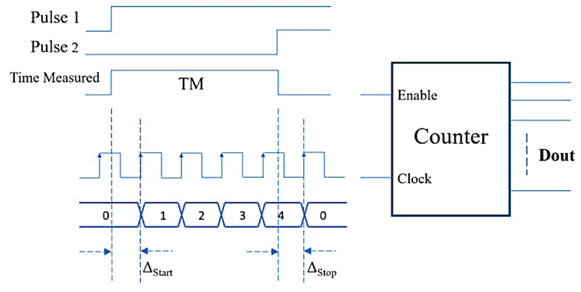
Figure 2.
Multi-Phase counter method.
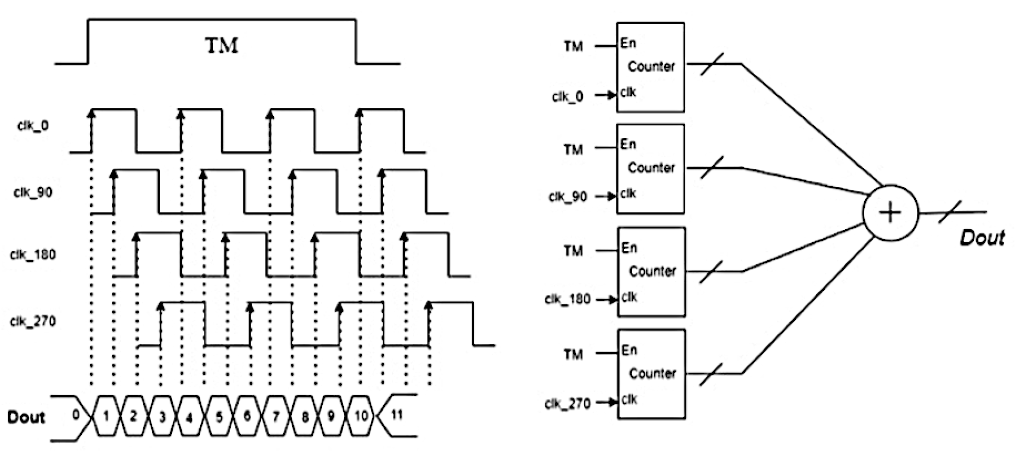
Figure 3.
Block diagram of 64 multi-phased 500MHz Clocks – TDC64.
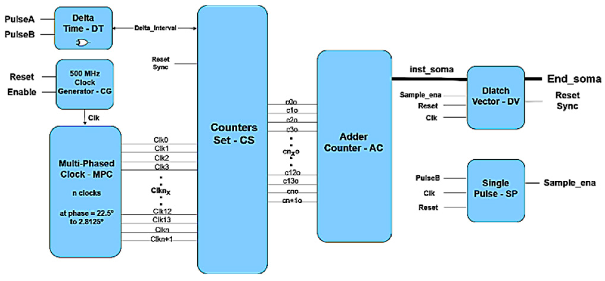
Figure 4.
The simulation results for a 300-nanosecond interval, yielding a total sum of 9600.
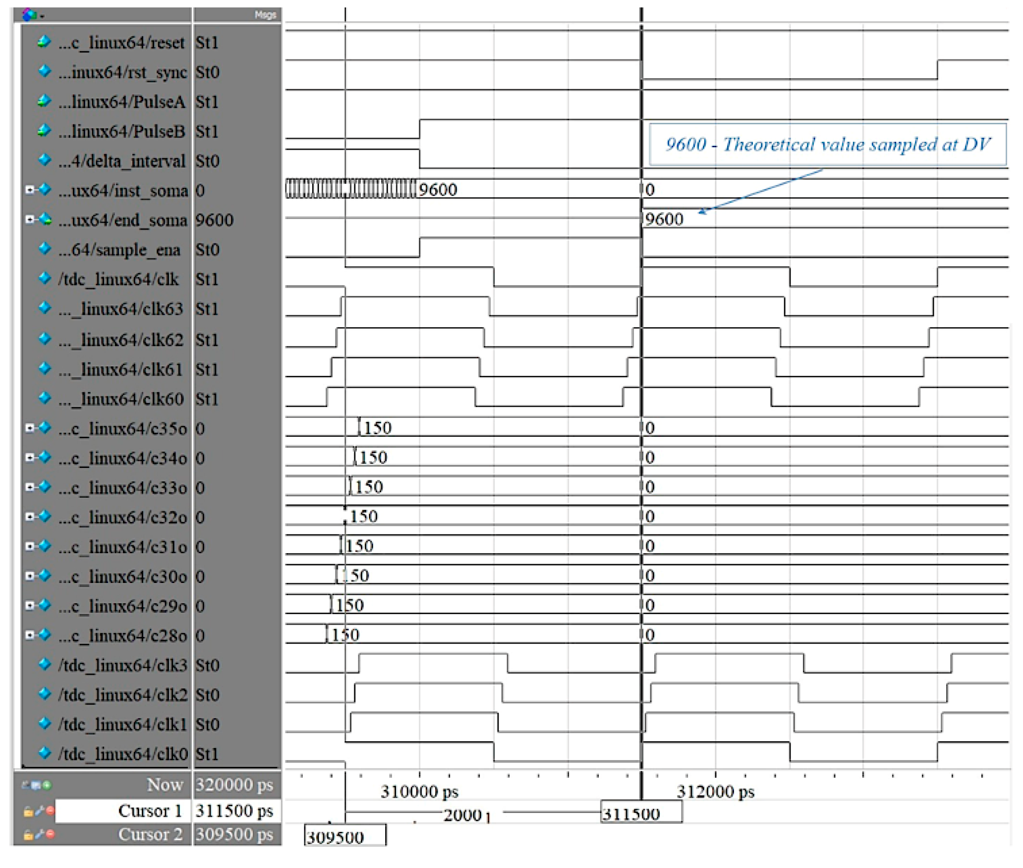
Figure 5.
Signal Tap result: 9660 at 300ns with less than 1% difference.
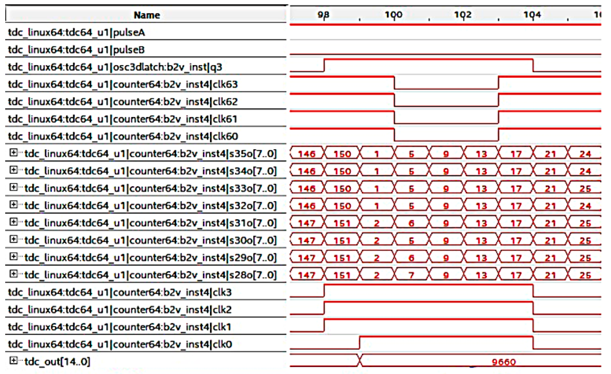
Figure 6.
Differential nonlinearity (a) and integral nonlinearity (b) on Signal Tap.
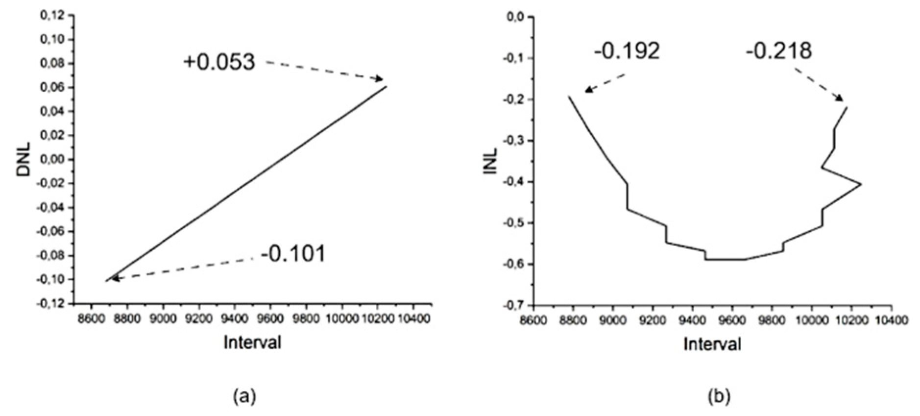
Figure 7.
External Signal generated on the waveform generator and extracted from the oscilloscope.
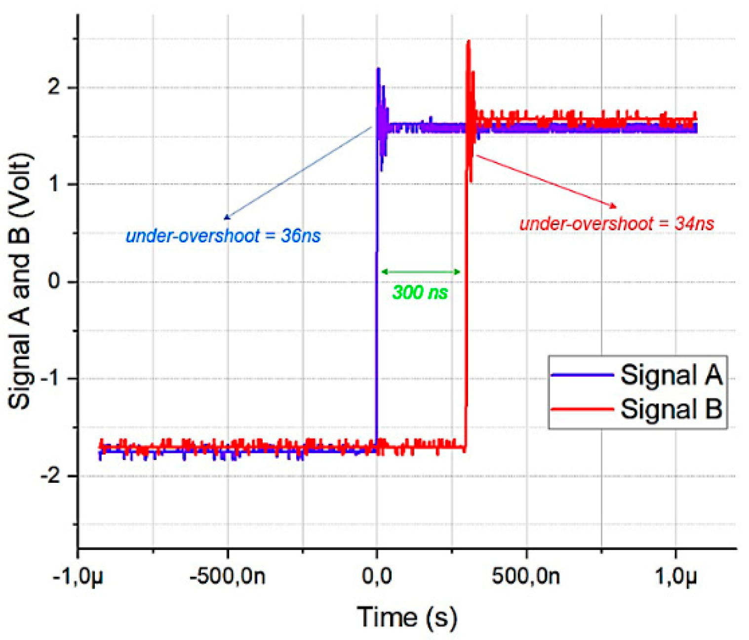
Figure 8.
External Signal generated on the waveform generator and extracted from the oscilloscope after mitigating noises.
Figure 8.
External Signal generated on the waveform generator and extracted from the oscilloscope after mitigating noises.
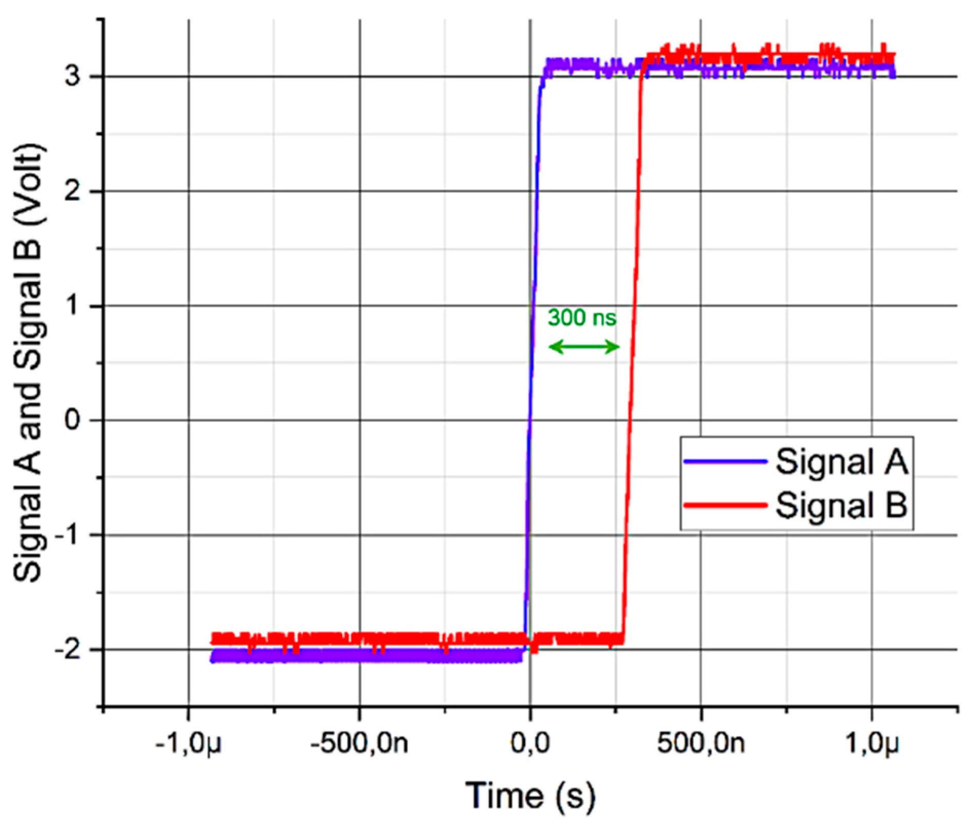
Figure 9.
Differential nonlinearity (a) and integral nonlinearity (b) on external signal without overshoot.
Figure 9.
Differential nonlinearity (a) and integral nonlinearity (b) on external signal without overshoot.
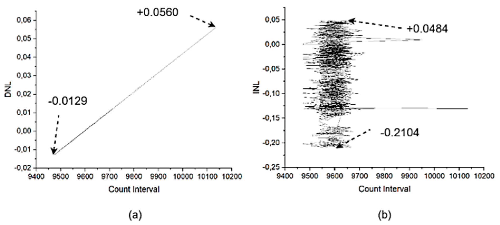
Figure 10.
Normalized Histogram Distribution with and without overshoot.
Disclaimer/Publisher’s Note: The statements, opinions and data contained in all publications are solely those of the individual author(s) and contributor(s) and not of MDPI and/or the editor(s). MDPI and/or the editor(s) disclaim responsibility for any injury to people or property resulting from any ideas, methods, instructions or products referred to in the content. |
© 2025 by the authors. Licensee MDPI, Basel, Switzerland. This article is an open access article distributed under the terms and conditions of the Creative Commons Attribution (CC BY) license (http://creativecommons.org/licenses/by/4.0/).
Copyright: This open access article is published under a Creative Commons CC BY 4.0 license, which permit the free download, distribution, and reuse, provided that the author and preprint are cited in any reuse.


