Submitted:
02 October 2025
Posted:
03 October 2025
You are already at the latest version
Abstract
This study presents a digitally-controlled, combined pulse-width and pulse-density modulator (DPWDM) that leverages the inherent pulse width modulation associated to natural binary counting. The proposed approach involves combining the individual bit-counting pulses to synthesize a modulated signal where the mean voltage is directly proportional to the input digital code. A circuit design, based on general-purpose components, is proposed for an 8-bit digital-to-analog converter. The architectural concept is scalable, supporting resolutions that can accommodate any number of bits. The paper describes the simulations conducted to verify the proper functioning of the circuit and to evaluate its performance. Tests were performed to determine the static characteristic of the converter, measure its nonlinearity, and observe its step response. The circuit combines the benefits of both PWM and PDM modulations, offering a blend of energy efficiency with simplicity and better smoothing.
Keywords:
pulse width modulator
; pulse density modulator
; digital-to-analog converter
; binary counter
1. Introduction
Pulse width modulation (PWM) and pulse density modulation (PDM) are two distinct digital-to-analog conversion techniques used to represent an analog signal using a series of pulses. While both methods utilize a binary signal (on/off pulses) to encode an analog value, their fundamental principles and applications differ significantly (see Figure 1).
Pulse width modulation is a digital signaling technique that varies the width of a square wave pulse to encode a specific analog value. The core principle of PWM is to maintain a constant frequency while adjusting the duty cycle. By rapidly switching the digital signal on and off at a high frequency, the average voltage across a load can be controlled, effectively simulating an analog output.
In contrast, pulse density modulation encodes the analog signal by varying the density of pulses over a fixed time interval. Unlike PWM, where the pulse width changes, PDM keeps the pulse width constant but adjusts the number of pulses within a given period. A higher analog value is represented by a higher density of pulses, whereas a lower value is represented by a sparser distribution of pulses. The average value of the signal is proportional to the number of pulses in the time window.
PWM is widely used in power control applications, such as motor speed control, dimming of LED lights, and voltage regulation in DC-DC converters. PDM, on the other hand, is most notably used in digital audio applications, particularly in single-bit delta-sigma converters found in microphones and speakers. PWM is generally more energy-efficient, as it typically involves fewer on/off transitions over the same time interval. PDM, however, offers advantages in terms of signal smoothing, as its spectral energy is spread across a wider frequency range.
The most common method for implementing a digital PWM signal is based on the direct digital emulation of a ramp waveform using a binary counter [1]. As depicted in Figure 2a, the counter’s ramp output is compared with the digital input code to establish the output signal’s duty cycle. A new modulation cycle begins when the counter wraps around. The counter’s full cycle, which has a duration of clock periods, determines the frequency of the modulated signal. This method provides excellent linearity; however, for applications requiring high sampling rates and high resolutions, the need for a very high-frequency clock becomes the primary limitation of this approach.
A faster alternative, based on a tapped delay line, is presented in [2]. As illustrated in Figure 2b, a brief pulse is injected into the delay line and propagates through its cells at a constant speed. The propagation ceases when the pulse reaches a selected tap, which in turn resets the output signal. The selection of the tap is made by a multiplex controlled by the digital input code, making the output signal’s duty cycle proportional to this code. A new modulation cycle begins when the traveling pulse loops around the entire line. The time required for the pulse to traverse the complete delay line determines the frequency of the modulated signal. While this method offers superior speed, its linearity is often compromised, as it is challenging to ensure a constant speed across a delay line with elements.
Regarding digital PDM modulators, the delta-sigma (ΔΣ) structure [1,3] has gained popularity in recent years. It employs oversampling techniques to achieve high resolution, albeit at the expense of increased latency and reduced bandwidth. Figure 3 shows the working diagram of a delta-sigma (ΔΣ) structure. The input is the digital code represented by the thickest line, and the output is the corresponding analog voltage. For explanatory purposes, we will assume that a signed representation is subtracted from a full-scale positive or negative number using the same number of bits. For example, an 8-bit incoming digital code, ranging from -128 to +127 as a signed integer, would be subtracted from -128 or +127, depending on the state of the feedback. The difference is applied to the input of an accumulator (the block). If the difference is positive, the output of the accumulator ramps up; if the difference is negative, the output of the accumulator ramps down. The MSB block selects the most significant bit of the word (the sign bit) and toggles the feedback state (and the output) whenever the accumulator causes the sign to change. This results in a PDM output waveform whose mean value is proportional to the input digital code.
There are alternatives to the delta-sigma structure, although they are only used in more specific scenarios. It is the case, for example, of the work published by Usui et al. [4], which proposes a DPDM modulator to drive organic light-emitting diode (AMOLED) displays based on a random dither matrix. The modulated signal, responsible for the dithering, is built by comparing the input digital code with a random number generated by a pseudo-uniform random source.
The digital PWDM modulation is a compromise between the PWM and PDM modulations that attempts to combine the advantages of both. On the one hand, it leads to less transitions than PDM to not compromise energy efficiency, particularly in power applications; and on the other hand, it spreads the spectral content of the PWM signal allowing for better filtering of the DC component.
The digital PWDM modulation splits the PWM signal into multiple, narrower pulses while maintaining its fundamental period and mean value. This approach yields a significant effect on both the time and frequency domains. In the time domain, the output filter’s smoothing element (the capacitor in Figure 2) charges and discharges more frequently and over shorter intervals, leading to a substantial reduction in the ripple of the output signal. Concurrently, in the frequency domain, the fundamental component is spread across higher frequencies, which increases the separation between the DC component and the spectral harmonics, thereby simplifying the smoothing process and relaxing the design requirements of the low-pass filter.
A good example of pulse manipulation while maintaining the mean value is the work of Crovetti [5]. The author distributes the pulses evenly over the signal period according to a predefined schedule based on dyadic sequences. The resulting PWDM signal is analyzed in both the time and frequency domains to conclude that the high-frequency spectral components are indeed attenuated and spread. This characteristic allows for a relaxation in the design requirements of the smoothing low-pass filter.
Another example of PWDM modulator is the work of Sheng et al. [6]. The authors rearrange the switching pulses according to predefined schedule in order to reduce current transients on a 20 kW inductively-coupled power transfer system.
This paper introduces a novel PWDM modulator that leverages the principles of binary counting for the temporal distribution of pulses, a distinct approach from reliance on a predefined schedule. This methodology effectively disperses the high-frequency spectral content of the modulated signal while rigorously preserving its mean value. Furthermore, this technique offers demonstrably greater simplicity and scalability when compared to previously cited methods [5,6].
The paper is organized as follows: Section 2 presents the new PWDM modulator and explains its operation working as a digital-to-analog (DA) converter; Section 3 describes the experimental tests conducted to validate the circuit and discusses the results obtained; and finally, Section 4 summarizes the main conclusions of the work.
2. Materials and Methods
The proposed circuit, shown in Figure 4, takes advantage of the pulse width created naturally by the binary counting sequence. Examining the binary counting sequence shown in Figure 5, we observe that the width of the pulses varies according to the bit’s weight. All bits generally have a pulse width of 50%, but this value is achieved through narrower pulses for the least significant bits and wider pulses for the more significant bits. The idea is to extract the first pulse of each bit - only the first occurrence - and combine them into a single signal. The result will be a width-density-modulated, binary-weighted pulse that can be used for DA conversion.
The extraction can be done by a simple logical circuit. For example, the narrower pulse, corresponding to the LSB, shall be collected if the input bit is true AND the output of the binary counter is . This leads to the top AND block shown in Figure 6, where the signal pulses with a width of if (where is the clock period of the binary counter). The same applies to the remaining bits:
- The pulse shall be collected if the corresponding input bit is true AND the output of the binary counter is , leading to signal in Figure 6.
- The pulse shall be collected if is true AND the output of the binary counter is , leading to signal in Figure 6.
- The pulse shall be collected if is true AND the output of the binary counter is , leading to signal in Figure 6.
Finally, all the collected pulses are summed by an OR gate to generate the PWDM output signal shown in Figure 6. The circuit can be optimized to use only negative gates, NAND and NOR, which are universal and faster. By applying De Morgan’s laws, we get:
which leads to the solution shown in Figure 7. This circuit exhibits three distinct processing levels irrespective of the number of bits being processed: a first level consisting of NOR gates, starting with inputs down to two inputs; a second level consisting of n 3-input NAND gates; and a third level composed of one n-input NAND gate, where n is the number of bits of the input code. This is always the case regardless of the number of bits, which makes this circuit very scalable.
As the number of bits increases, diode resistor logic can be used to implement NOR gates with many inputs. Figure 8 shows a 15-input NOR gate where the delay is mainly determined by the NOT gate. A similar arrangement can be done for the NAND gate at the third level. Looking again at Figure 7, assuming a propagation delay of 15 ns for each of the three processing levels, the cumulative delay in generating the PWDM signal remains consistently at 45 ns, independent of the number of bits processed. The biggest source of delay in the PWDM modulator is not the pulse extraction logic, but the fact that it takes a full binary count to do the conversion, i.e., clock pulses. As n increases, the modulation rate must be relaxed or the clock rate of the binary counter must be increased.
To obtain an analog voltage, the PWDM signal must pass through a low-pass filter to recover its mean value. In Figure 4, this is achieved through a Sallen-Key active filter exhibiting Butterworth response. Alternative filter topologies (active or passive) and filter responses (such as Chebyshev or Elliptic) are also viable options for this purpose.
3. Results and Discussion
This section details the simulations performed to verify the proper functioning of the circuit and to evaluate its performance. The simulations were done using NI Multisim v14.3 running on a computer characterized by Intel(R) Core(TM) i7-8550U CPU @ 1.80 GHz, 16 GB RAM, and Windows 11 Home 64 bits. The simulation protocol encompassed the following tests:
- PWDM operation.
- Static transfer characteristic (output voltage versus input digital code in steady state).
- Differential nonlinearity (DNL).
- Step response.
The discussion will commence with a detailed description of the circuit under test, followed by an individualized explanation of each simulation carried out.
3.1. Circuit Under Test
The circuit under test, shown in Figure 4, is an 8-bit DA converter that includes an 8-bit binary counter, a PWDM modulator, and an optional smoothing filter to provide an analog output voltage. The PWDM modulator’s architecture is analogous to that depicted in Figure 7, with the exception that it has been scaled up to 8 bits. Internally, it is implemented using push-pull CMOS gates that operate at 5 V and exhibit propagation delays of 15 ns for both high-to-low and low-to-high transitions. The clock source and the 8-bit counter were idealized to facilitate a performance evaluation focused exclusively on the custom-designed circuit elements, namely the PWDM modulator and the smoothing filter.
Each conversion takes 256 clock cycles to complete, which corresponds to 4 s per conversion. Higher conversion rates imply higher clock frequencies.
The smoothing filter works around the OPA2340, which is a general-purpose operational amplifier optimized for low-voltage, rail-to-rail operation. The circuit is designed to have a Butterworth response with a cutoff frequency equal to 10 kHz and a stationary gain equal to one. The cutoff frequency is appropriate for a wide range of industrial applications and is substantially lower than the conversion rate, which is critical for providing a well-smoothed analog output voltage.
3.2. PWDM Operation
The digital code was applied to the input of the PWDM modulator to validate its functionality. This specific sequence was chosen because it generates a wide variety of pulses, allowing for a comprehensive assessment of the modulator’s performance. Figure 9 displays the corresponding output signal. Each ’1’ bit contributes to an increase in the output’s duty cycle, commencing with the LSB that generates the narrowest pulse and culminating with the MSB responsible for the widest pulse. The signal’s amplitude spans the full rail-to-rail range, from 0 V to 5 V. A complete conversion cycle is executed within 4 s, as expected. It is important to note that duty cycle never reaches 100% because the PWM line goes down during one clock period when the binary counter returns to zero.
It is also important to analyze the spectral signature of the PWDM signal. Figure 10 shows the amplitude spectrum of the PDWM signal shown in Figure 9 (left) and compares it with the amplitude spectrum of an “equivalent” PWM signal with the same duty cycle but only one switching edge (right). As expected, the DC component is the same for both signals (68%), but the first harmonic is significantly lower, 2.17 V versus 2.71 V, which leads to an attenuation equal to . This "extra" attenuation adds to that of the smoothing filter and leads to less ripple in the output voltage. The more switching edges the PWDM signal has, the more energy is transferred to the high frequencies. Of course, this improvement depends on the digital sequence at the input, but it exists and is noticeable.
3.3. Static Transfer Characteristic
The static transfer characteristic of the DA converter was determined by sequentially applying the complete set of binary input combinations and recording the corresponding output voltage values under steady-state conditions.
Table 1 presents the output voltage () obtained for a selection of binary input combinations, specifically encompassing the minimum (all zeros), maximum (all ones), and power-of-two codes. The graphical representation of the static transfer characteristic is illustrated in Figure 11, with the abscissa representing the input digital code (expressed as an integer value) and the ordinate representing the corresponding mean output voltage. The observed characteristic exhibits a high degree of linear correlation (R=1) with a fitted straight line characterized by a slope of 19.547 mV/LSB and an offset of 1.1119 mV. According to [7], these values are the independently based gain and offset of the DA converter, respectively.
3.4. Differential Nonlinearity (DNL)
The DNL measures the difference between the measured and the ideal output voltages for successive digital codes [8]. It can be expressed as a fraction of the LSB as follows:
where i represents the ith digital code.
The output voltage measurements obtained during the static characterization were applied to Equation 2, and the resulting data is presented graphically in Figure 12. It is clear that the DNL remains below 1 LSB, thereby confirming the absence of missing codes in the converter’s transfer characteristic. Some performance degradation is also observed for larger digital codes, which is understandable because any deviations in pulse width have a greater impact on the output voltage.
3.5. Step Response
The step response is an effective tool for identifying a system’s dynamic properties [9]. Following this idea, a sharp transition was made to the input, switching the digital code from 0000 0000 to 1000 0000, and the accompanying output voltage was measured over time. Figure 13 shows the resulting transitory behavior.
Observation of the converter’s dynamic response reveals that it is primarily governed by the second-order low-pass Butterworth filter. The curve is characterized by an overshoot of 4%, a rise time close to 51.8 s, and a stationary gain equal to one. These values correspond to a damping factor of 0.707 and a natural frequency of 10 kHz, as expected. It should be noted that the Butterworth characteristic is often the preferred choice for smoothing filters due to its optimal balance between overshoot and speed, enabling the fastest transient response without excessive ringing.
4. Conclusions
The paper presented a PWDM modulator that leverages on the inherent pulse width modulation associated to natural binary counting. The core concept is the combination of individual bit-counting pulses to synthesize a modulated signal where the mean voltage is directly proportional to the input digital code. A circuit capable of executing this function was presented using general-purpose components. The circuit design is highly scalable to accommodate any number of bits; however, it is crucial to note that increasing the modulator’s resolution will result in a longer processing time and a reduction in bandwidth.
The PWDM modulator was tested to validate its functionality and to assess its performance as a digital-to-analog converter. The modulator operated as expected, generating multiple pulses over a sampling period, which translates to a spreading and attenuation of the high-frequency components. As a digital converter, the circuit demonstrated negligible gain and offset errors, no missing codes, and a dynamic performance dominated by a second-order low-pass Butterworth filter with a 10 kHz bandwidth.
Funding
This research received no external funding.
Conflicts of Interest
The authors declare no conflicts of interest.
References
- Adrian, V.; Gwee, B.H.; Chang, J.S. A review of design methods for digital modulators. In Proceedings of the IEEE International Symposium on Integrated Circuits (ISIC-2007), Singapore, 26-28 September 2007. [Google Scholar]
- Syed, A.; Ahmed, E.; Maksimovic, D.; Alarcón, E. . Digital pulse width modulator architecture. In Proceedings of the 3IEEE 35th Power Electronics Specialists Conference (ISIC-2007), Aachen, Germany, 20-25 June 2004. [Google Scholar]
- Enuchenko, M.; Korotkov, A. . Digital-to-analog converters based on delta-sigma modulators. Journal of Communications Technology and Electronics 2022, 67, 1–16. [Google Scholar] [CrossRef]
- Usui, T.; Nakajima, Y.; Shiga, T. . A digital driving method using pulse-density modulation with a random dither matrix for higher motion image quality. Journal of the Society for Information Display 2022, 30, 198–208. [Google Scholar] [CrossRef]
- Crovetti, P. . All-digital high resolution D/A conversion by dyadic digital pulse modulation. IEEE Transactions on Circuits and Systems 2017, 64, 573–584. [Google Scholar] [CrossRef]
- Sheng, X.; Shi, L.; Fan, M. . An improved pulse density modulation of high-frequency inverter in ICPT system. IEEE Transactions on Industrial Electronics 2021, 68, 8017–8027. [Google Scholar] [CrossRef]
- IEEE Standard for digitizing waveform recorders (IEEE 1057-2017); IEEE Standards Association: NJ, USA, 2017.
- Understanding data converters (application report). Available online: www.ti.com/lit/an/slaa013/slaa013.pdf (accessed on day month year).
- Liu, T.; Wang, Q.G.; Huang, H.P. . A tutorial review on process identification from step or relay feedback test. J. Process Control 2013, 23, 1597–1623. [Google Scholar] [CrossRef]
Figure 1.
Pulse width versus pulse density modulations: (a) PWM. (b) PDM.
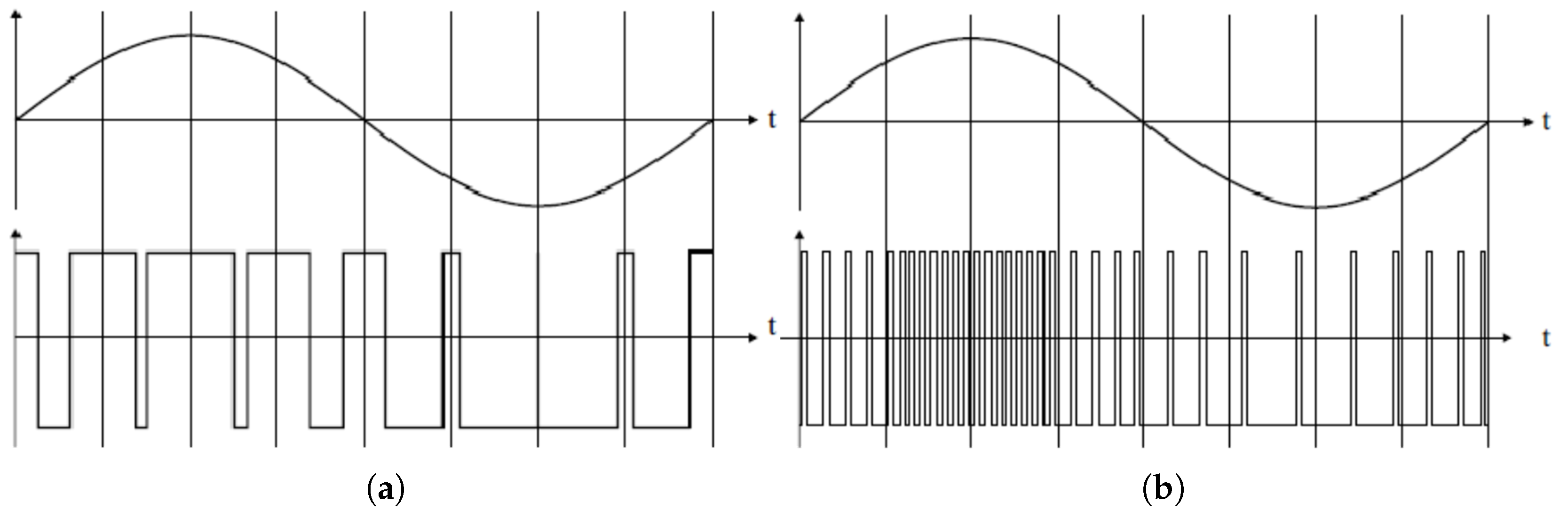
Figure 2.
Digital PWM generators: (a) Comparison with a ramp waveform. (b) Tapped delay line approach.
Figure 2.
Digital PWM generators: (a) Comparison with a ramp waveform. (b) Tapped delay line approach.
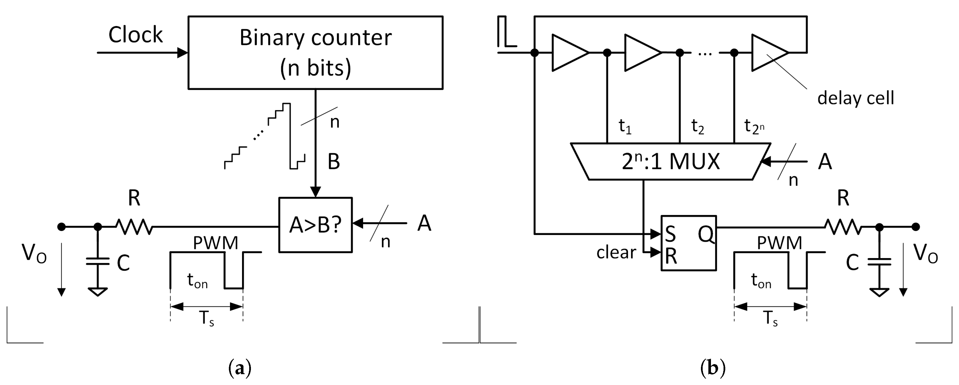
Figure 3.
ΔΣ structure.
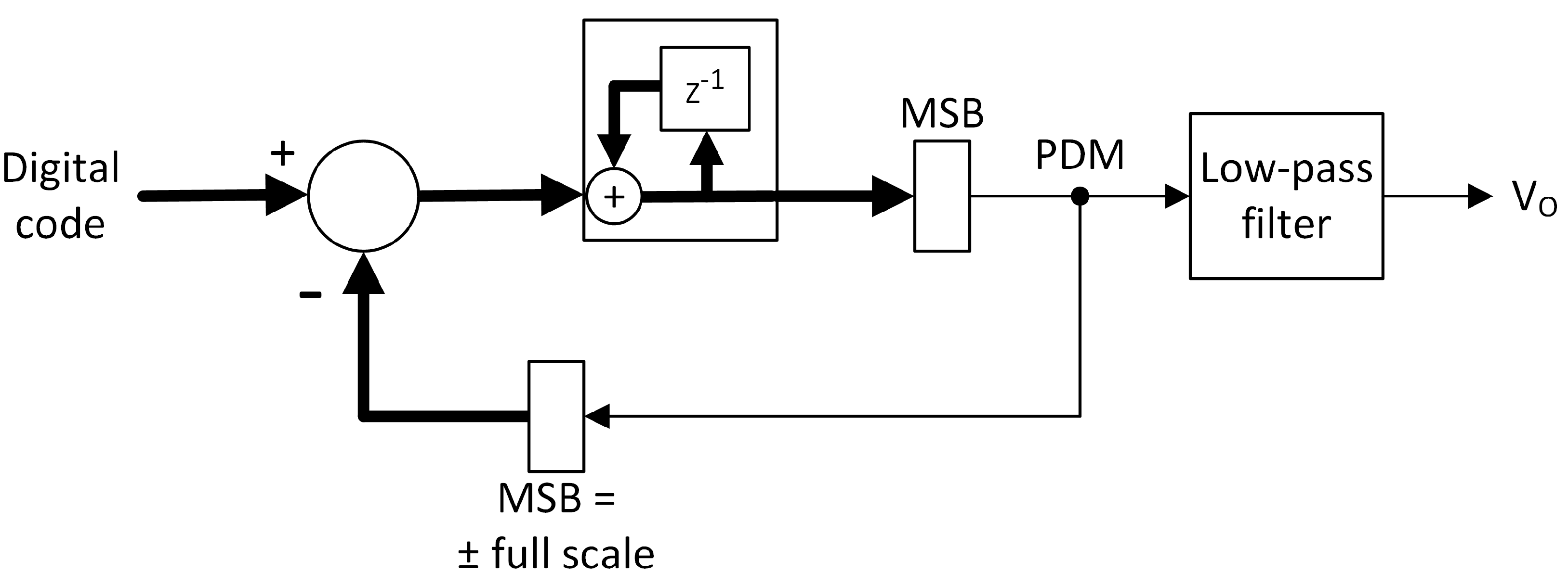
Figure 4.
8-bit DAC based on PWDM modulation. The input digital code is , with being the most significant bit (MSB) and the least significant bit (LSB). The output is provided as a pulse-width-density modulated signal (signal PWDM) or as an analog voltage (signal ).
Figure 4.
8-bit DAC based on PWDM modulation. The input digital code is , with being the most significant bit (MSB) and the least significant bit (LSB). The output is provided as a pulse-width-density modulated signal (signal PWDM) or as an analog voltage (signal ).
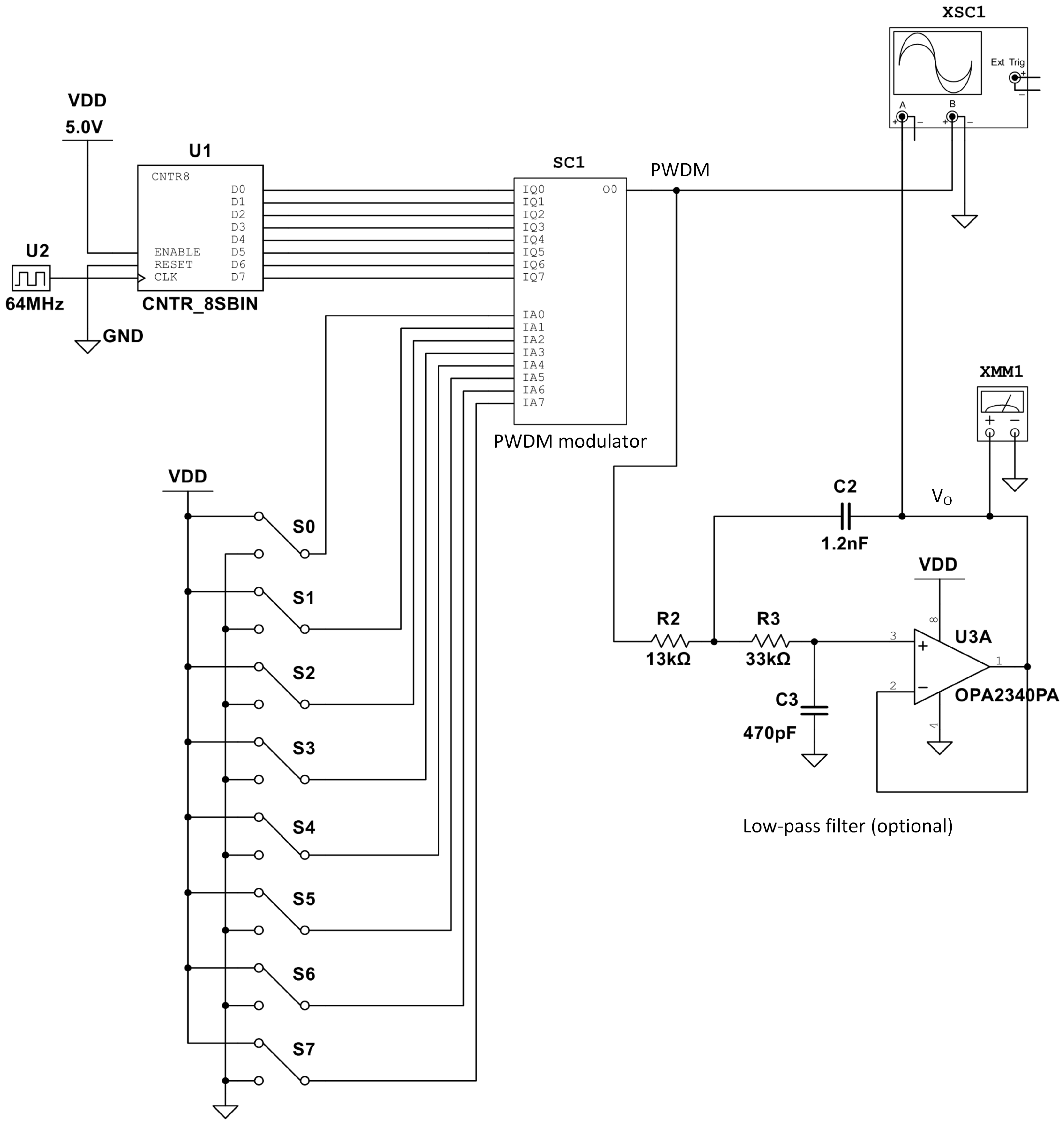
Figure 5.
Output of the binary counter. The width of the pulses increases as a power of 2.
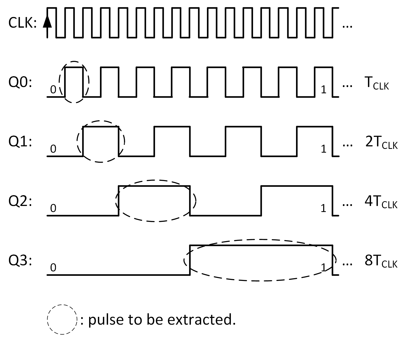
Figure 6.
Pulse extraction from the LSB () to the MSB () followed an OR gate.
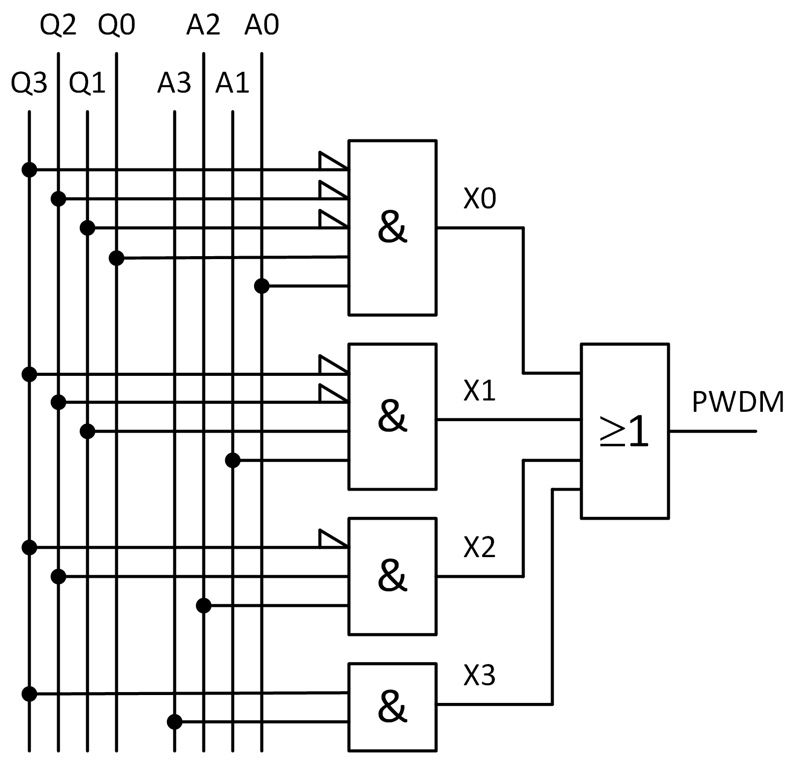
Figure 7.
Optimized pulse extraction using only NAND and NOR gates.
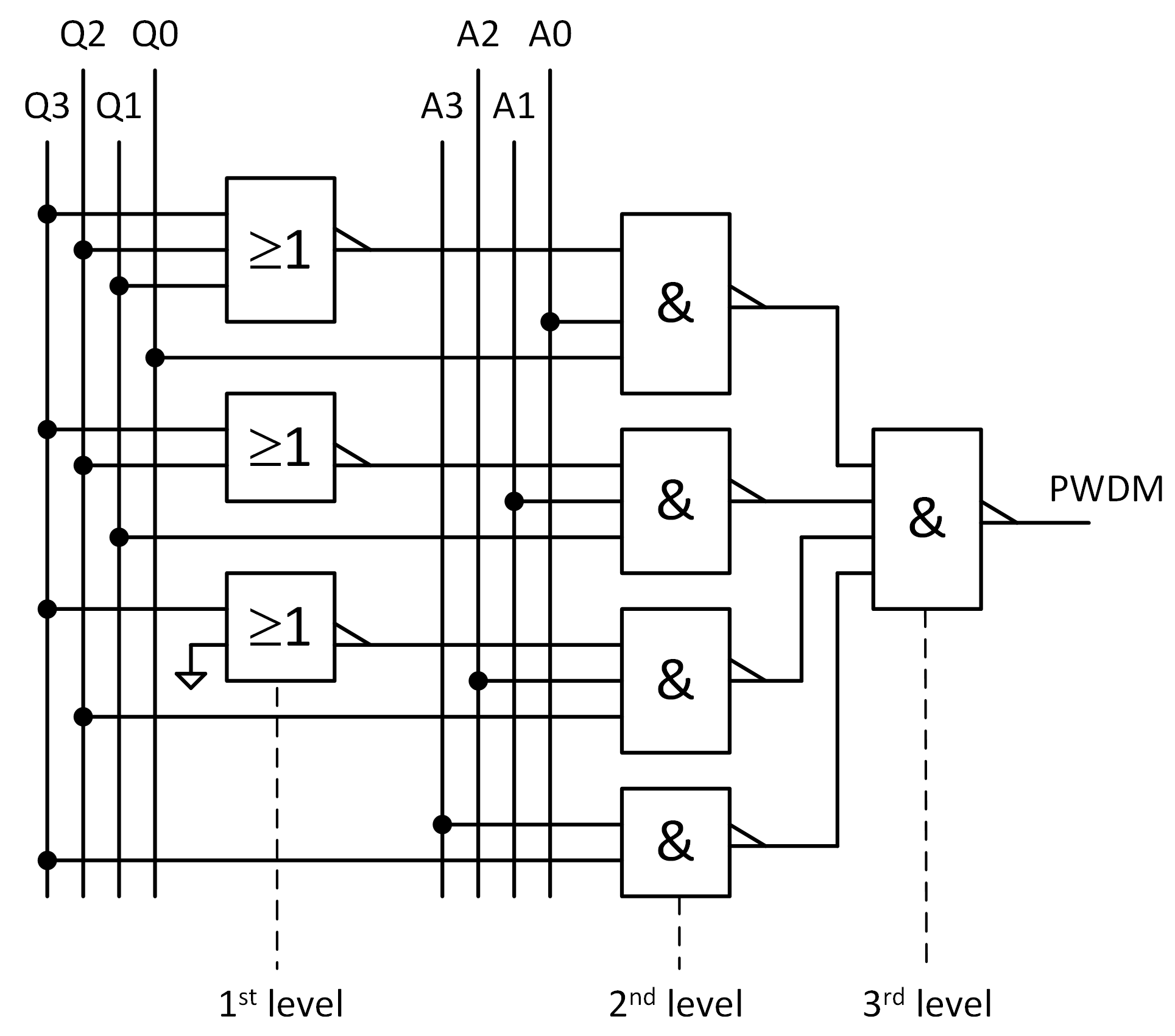
Figure 8.
15-input NOR gate.
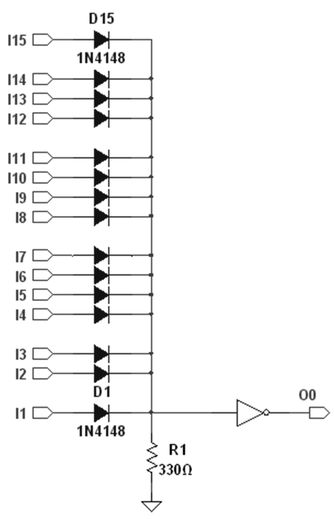
Figure 9.
PWDM signal for the input digital code 1010 1101. The duty cycle is .
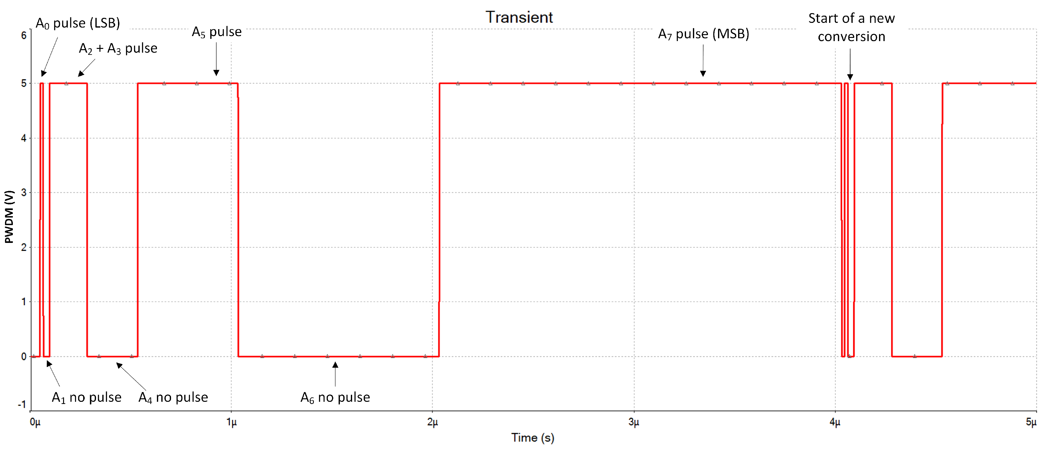
Figure 10.
Spectrum comparison between PWDM and PWM signals: (a) Amplitude spectrum of the PWDM signal shown in Figure 9. (b) Amplitude spectrum of an "equivalent" PWM signal.
Figure 10.
Spectrum comparison between PWDM and PWM signals: (a) Amplitude spectrum of the PWDM signal shown in Figure 9. (b) Amplitude spectrum of an "equivalent" PWM signal.
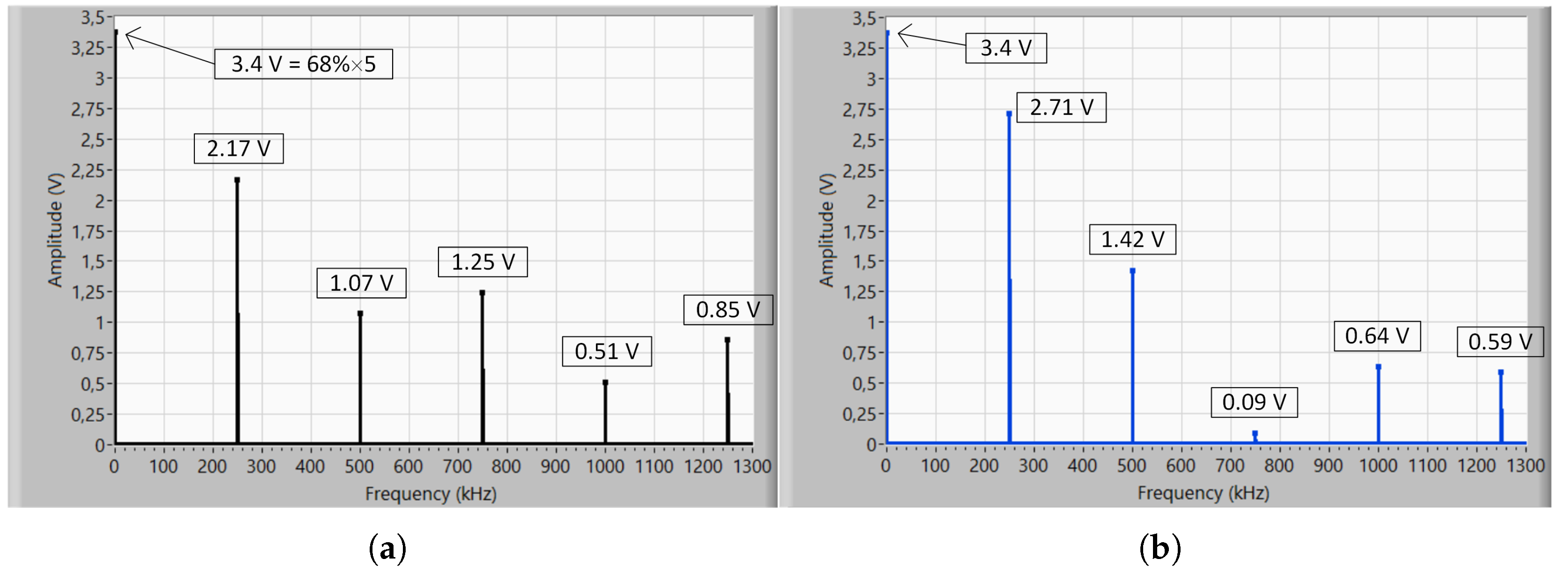
Figure 11.
Static transfer characteristic.
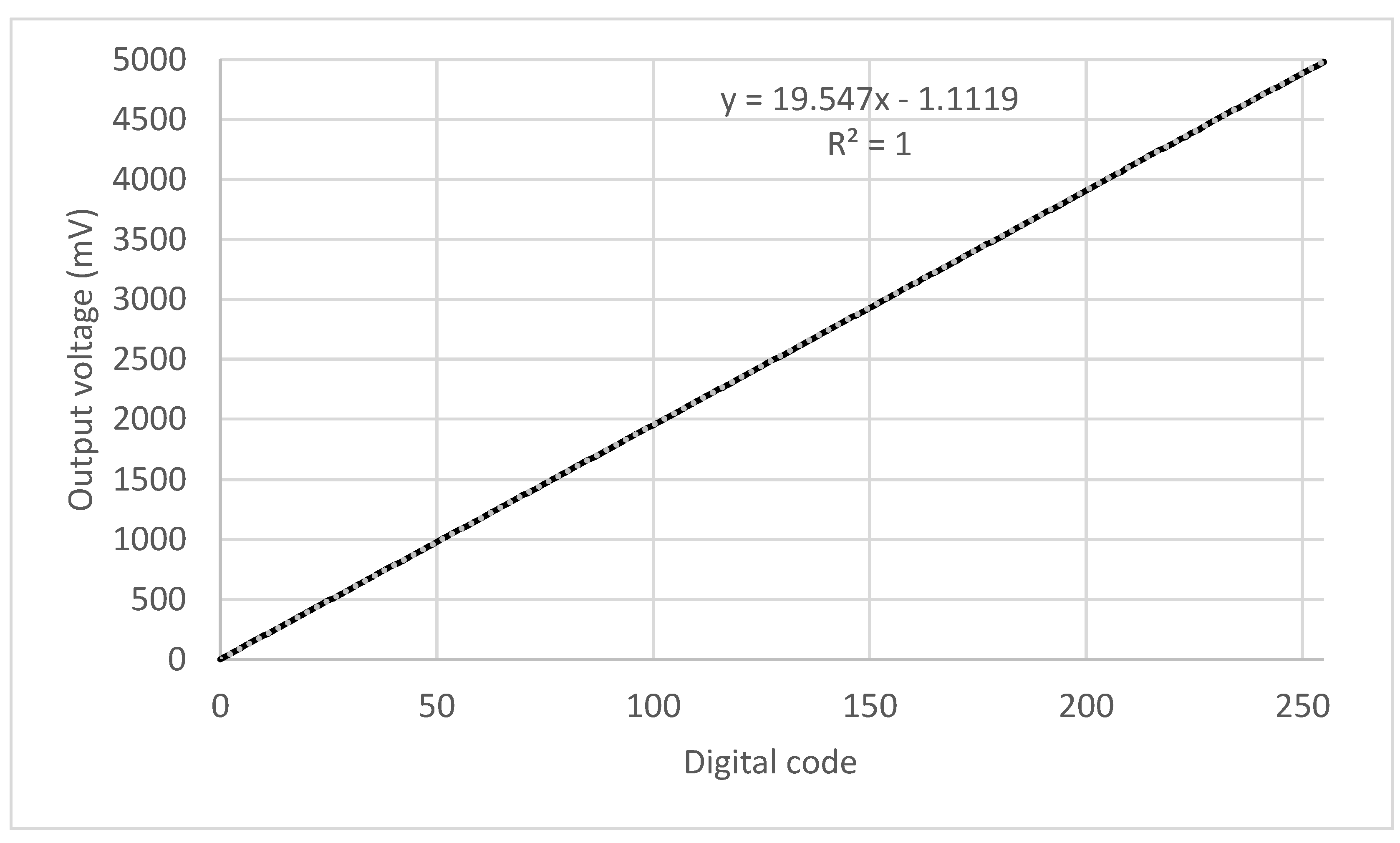
Figure 12.
Differential nonlinearity.
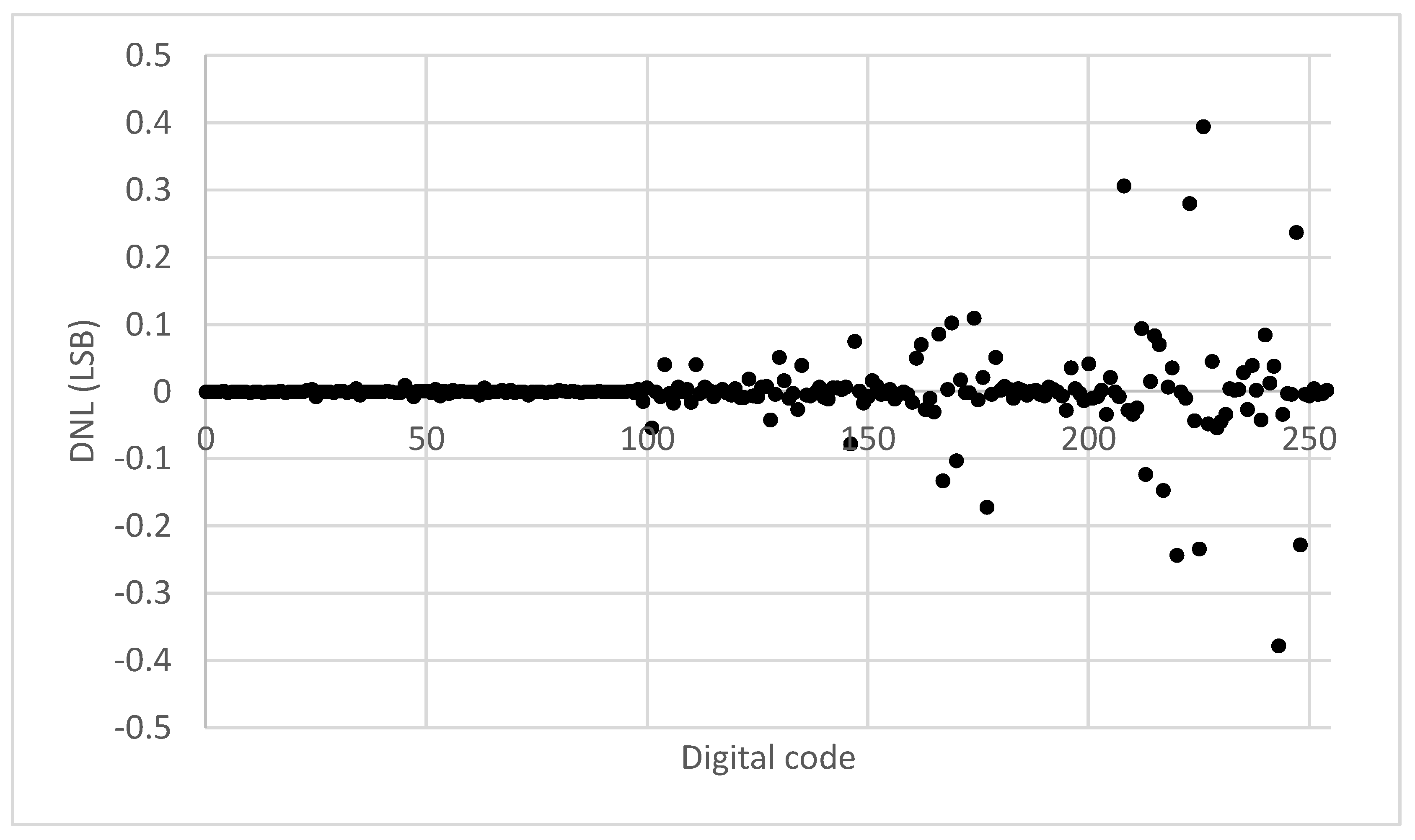
Figure 13.
Step response.
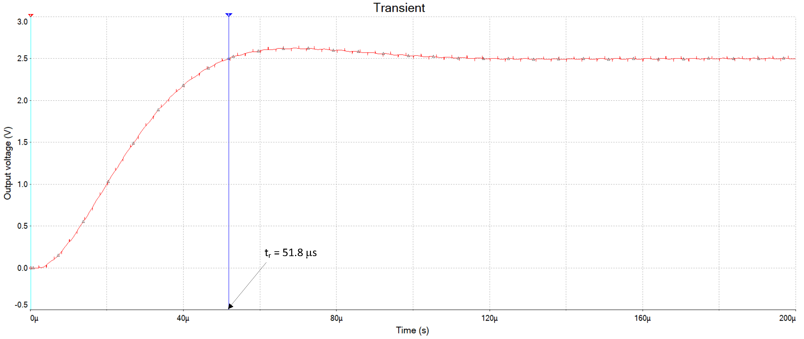

Table 1.
Values of the static transfer characteristic.
| Input digital code | (V) |
|---|---|
| 0000 0000 | 2 |
| 0000 0001 | 19.531m |
| 0000 0010 | 39.068m |
| 0000 0100 | 78.135m |
| 0000 1000 | 156.264m |
| 0001 0000 | 312.511m |
| 0010 0000 | 625.022m |
| 0100 0000 | 1.25012 |
| 1000 0000 | 2.49998 |
| 1111 1111 | 4.98080 |
Disclaimer/Publisher’s Note: The statements, opinions and data contained in all publications are solely those of the individual author(s) and contributor(s) and not of MDPI and/or the editor(s). MDPI and/or the editor(s) disclaim responsibility for any injury to people or property resulting from any ideas, methods, instructions or products referred to in the content. |
© 2025 by the authors. Licensee MDPI, Basel, Switzerland. This article is an open access article distributed under the terms and conditions of the Creative Commons Attribution (CC BY) license (http://creativecommons.org/licenses/by/4.0/).
Copyright: This open access article is published under a Creative Commons CC BY 4.0 license, which permit the free download, distribution, and reuse, provided that the author and preprint are cited in any reuse.


