1. Introduction
β-Ga₂O₃ has emerged as a prominent candidate for next-generation semiconductor materials, particularly in power electronics applications. Its appeal arises from two key attributes: an ultrawide bandgap (~4.9 eV) and the relative ease of achieving n-type doping [
1,
2,
3,
4,
5]. These characteristics distinguish
β-Ga₂O₃ from other wide-bandgap semiconductors such as aluminum nitride (AlN) and diamond[
6,
7]. Recent advancements in melt-grown synthesis techniques have enabled the fabrication of bulk
β-Ga₂O₃ crystals with diameters ranging from 6 to 8 inches [
8,
9,
10], positioning this material as a cost-effective option for scalable production. Nonetheless, the absence of stable p-type conductivity remains a critical challenge for its full technological implementation [
9,
11]. This limitation stems from difficult to introduce common acceptor elements with ionization energies of less than 1 Ev [
12], which inherently restricts the formation of effective p-type conductivity.
To address the challenge of p-type conductivity in
β-Ga₂O₃, researchers have explored heterojunctions with other p-type oxide semiconductors, such as nickel oxide (NiO) [
1,
13,
14,
15] and chromium trioxide (Cr₂O₃) [
16,
17], achieving significant advancements in device robustness and breakdown voltage. For instance, Ye, et al. [
1] achieving significant advancements in device robustness and breakdown voltage. Several groups have further reported NiO/Ga₂O₃ rectifiers with high temperature blocking capabilities (8 kV) [
14,
18,
19]. More recently, Su et al. [
16] fabricated a p-Cr₂O₃/
β-Ga₂O₃ heterojunction diode exhibiting a high ideality factor of 1.07 at 1.96 kV. Despite these advances, critical challenges persist in heterojunction integration, including lattice mismatch (for NiO/
β-Ga₂O₃ is around 7.6% and for α-Ga2O3/
β-Cr2O3 is around 5.9% [
17,
20]), crystallographic difference, and conduction band offset discrepancies [
21]. These limitations hinder the realization of defect-free interfaces and optimal device performance.
Homoepitaxial p-type
β-Ga₂O₃ is highly desirable for power and optoelectronic devices, yet conventional dopants such as Mg and Zn introduce deep traps (>1 eV) that pin the Fermi level and prevent hole activation [
12,
22], making the material resistive [
23]. This difficulty is further driven by the oxygen 2p-dominated valence band, which limits hole transport [
24]. To overcome this, Li et al. [
25] fabricated Cu-doped p-type
β-Ga₂O₃ through liquid-metal printing, Horng et al. [
21,
26] achieved p-type conductivity by phosphorus implantation enabling PN diodes, and our group[
4] realized Se–Mg co-doping via ion implantation, where Se raises the valence band to reduce Mg activation energy[
24,
27]. However, these approaches lack potential for scalability. Therefore, epitaxial growth remains critical for achieving practical p-type
β-Ga₂O₃ and enabling device integration.
This work presents a Te–Mg co-doping strategy to enable p-type conductivity in homoepitaxial β-Ga₂O₃ grown by metal–organic chemical vapor deposition (MOCVD). Hall measurements reveal a room-temperature resistivity as low as 32.4 Ω·cm with a corresponding hole concentration of 1.78 × 10¹⁷ cm⁻³, while the highest hole mobility of 5.29 cm² V⁻¹ s⁻¹ is achieved at a carrier concentration of 5.72 × 10¹⁴ cm⁻³. A positive Seebeck coefficient further confirms p-type conduction.
3. Results and Discussion
Prior to homoepitaxial growth on β-Ga₂O₃ substrates, two heteroepitaxial samples (S1 and S2) were grown on (0001) sapphire substrates using metal-organic chemical vapor deposition (MOCVD) with Te-only (S1) and Te-Mg co-doping (S2). These samples were grown with triethylgallium (TEGa) and O₂ as the Ga and oxygen sources, respectively. Diethyltellurium (DETe) served as the Te source while bis(cyclopentadienyl)magnesium (Cp₂Mg) was introduced as the Mg source in S2. S1 utilized only DETe, establishing a baseline for Te-only doping. All the films were deposited with thickness controlled at 300 nm.
As summarized in
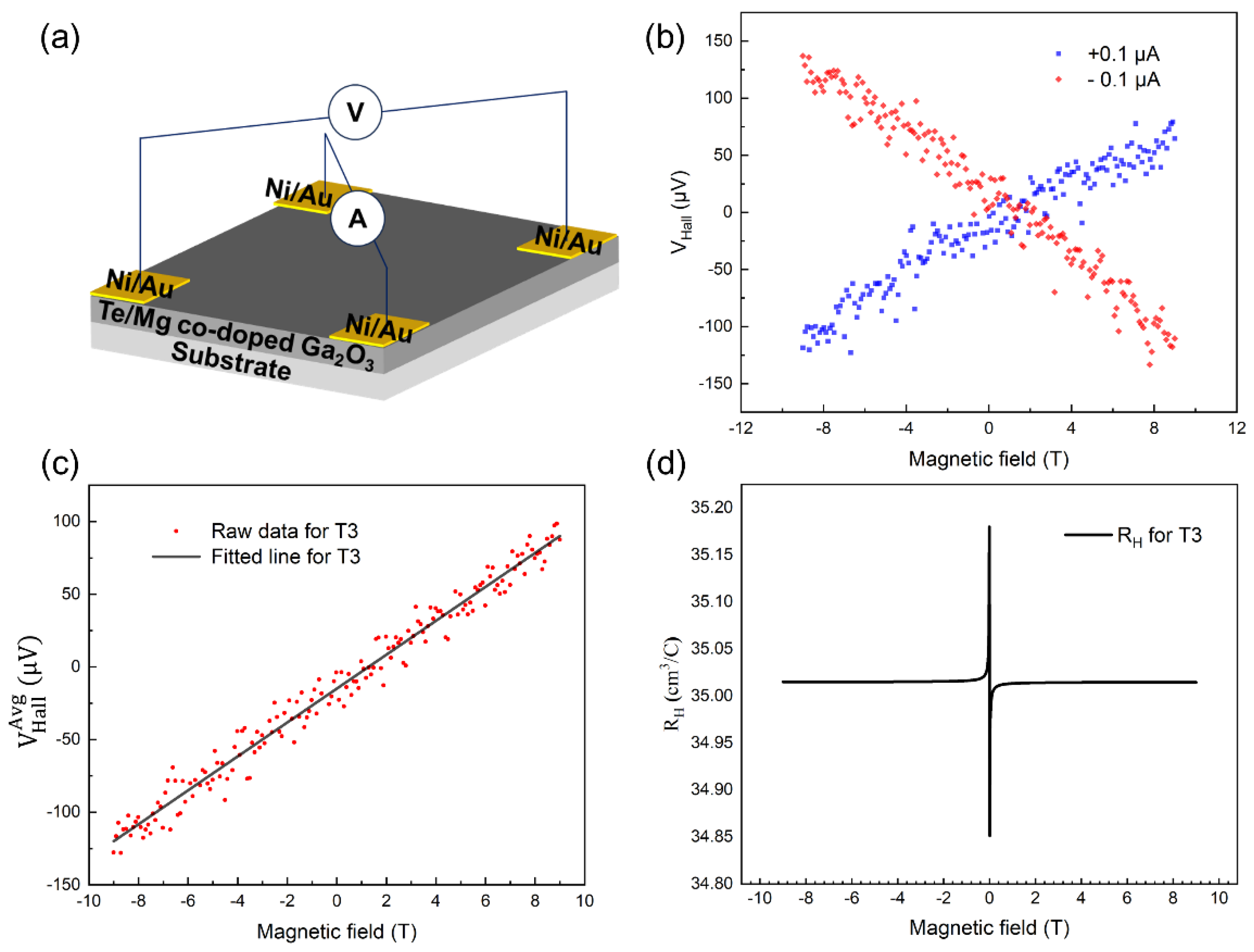
Table 1, S2 exhibited significantly lower resistivity compared to S1, underscoring the role of Mg co-doping in enhancing electrical conductivity. Hall effect measurements in a van der Pauw configuration (Toho HL-9900) using direct current (DC) mode and magnetic field of ±1.5 T, performed using 20 nm/60 nm Ni/Au contacts, confirmed these trends (
Figure 1a). Prior to Hall measurements, current-voltage (I-V) profiling verified Ohmic behavior of the contacts, as demonstrated in supplementary materials
Figure S1.
Building on these results, three Te-Mg co-doped
β-Ga₂O₃ thin films (T1–T3) were grown on insulating Fe-doped
β-Ga₂O₃ (010) substrates under near-identical MOCVD conditions, with 300 nm thickness. Growth parameters are kept in confidentiality attributed to commercial purpose. Partial growth conditions and room-temperature (RT) Hall results for T1–T3 are detailed in
Table 1.
To confirm the validity of the results, we conducted temperature-dependent Seebeck measurement for sample S2 and Hall measurement with varied magnetic field for sample T3, as shown in
Figure 1 and
Figure 2.
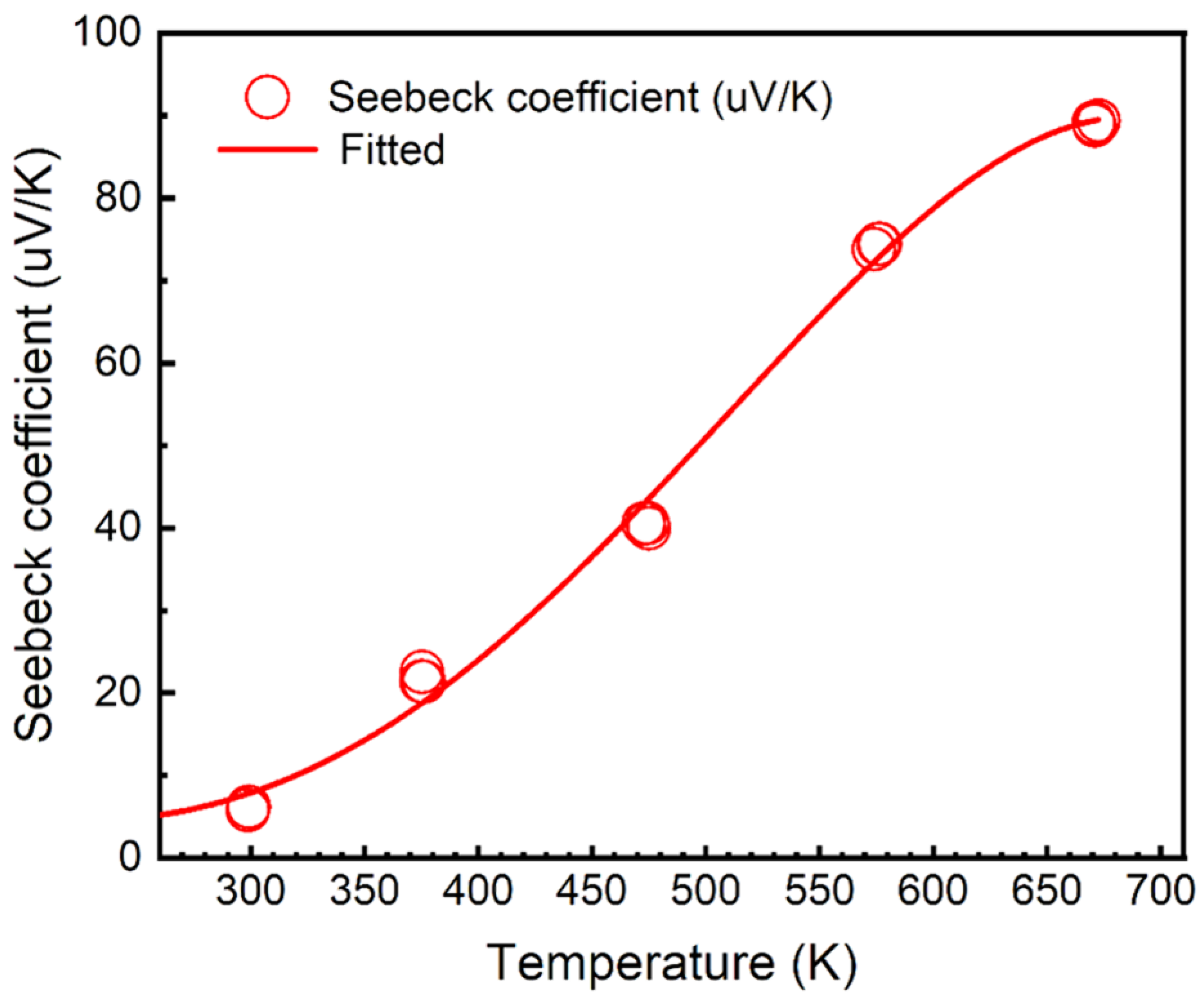
The temperature-dependent Seebeck measurement was conducted from room temperature to 674.15K (400℃) using a Thermoelectric Material Testing System (Cryoall CTA-3). The temperature gradient (ΔT) was set constant at 3K. As the results in
Figure 1, where the Seebeck coefficient (S) is determined by
, S remains positive and increases with the overall temperature, indicating that S2 was a p-type semiconductor.
For sample T3, Hall measurement was conducted with magnetic field varied from -9 T to 9 T with an interval of 0.02 T, as shown in
Figure 1(b)-1(d). The measurement was conducted using a Physical Property Measurement System (PPMS, Quantum Design) connected with external source meters (Keithley 6221 as DC source and Keithley 2182a as voltage monitor).
Figure 1(b) shows the Hall voltage (V
Hall) under positive (+0.1μA,
) and negative bias (-0.1μA,
) with varying magnetic fields. To eliminate thermoelectric voltage and misalignment, the V
Hall in
Figure 1(c) is acquired by averaging the results from
Figure 1(b) (
). As depicted in
Figure 1(c), the Hall voltage exhibited positive values under positive magnetic fields and negative values under negative magnetic fields, indicative of p-type conduction behavior.
Figure 1(c) reveals nearly identical Hall coefficients of approximately 35.02 cm³/C. The Hall mobility and carrier concentration are deduced to be 1.08 cm
2/V⸱s and 1.78×10
17 cm
-3 respectively, consistent with the prior findings presented in
Table 1.
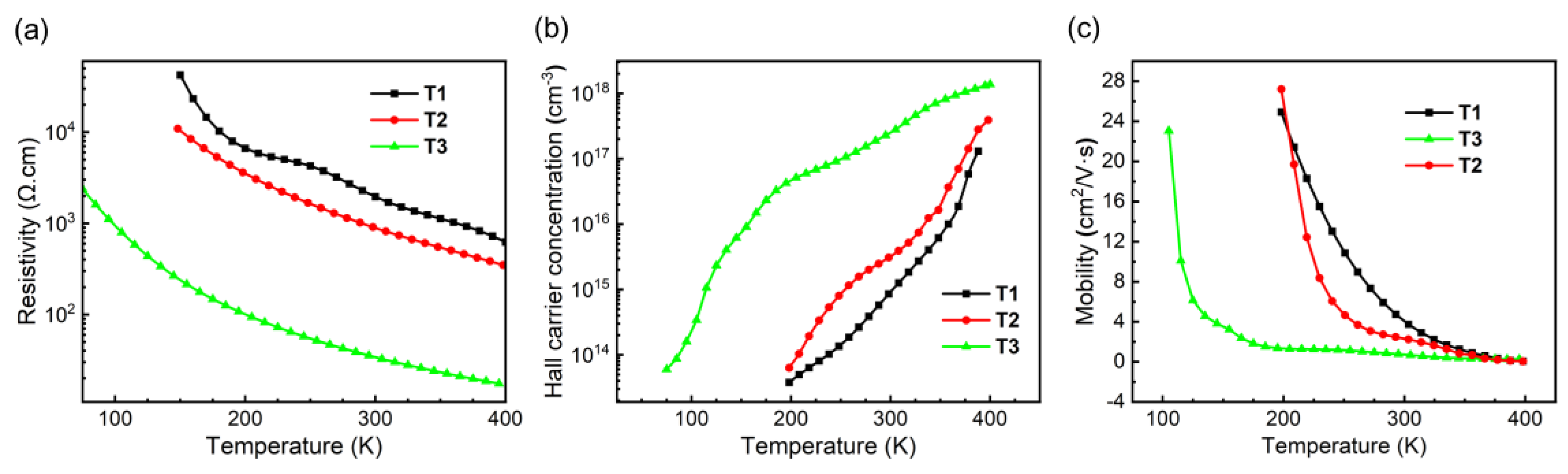
Temperature-dependent Hall measurements were performed on homoepitaxial samples T1, T2, and T3 to evaluate their electrical properties, with van der Pauw configuration (Toho HL-9900) using DC mode and magnetic field of ±1.5 T, as shown in
Figure 2. During measurement, Ohmic contacts were confirmed via IV profiling at 200 K for T1 and T2, and at 75 K for T3. As shown in
Figure 2(a)–2(c), increasing Te doping concentration correlates with a decrease in resistivity (ρ) and Hall carrier concentration (n
H), alongside a reduction in hole mobility (μ
H). These trends align with typical semiconductor behavior: higher doping introduces more charge carriers (n
H), which reduces resistivity (ρ), while enhanced ionized impurity scattering lowers mobility (μ
H). Notably, sample T3, with the highest Te doping, exhibits the lowest resistivity (32.4 Ohm·cm) and highest carrier concentration (1.78 × 1017 cm⁻³ at RT), albeit with significantly reduced mobility (1.08 cm²/V·s). In contrast, sample T1, with the lowest Te content, achieves a high hole mobility of 5.29 cm²/V·s at RT and 24.93 cm²/V·s at 200 K, suggesting reduced scattering at cryogenic temperatures. The abrupt resistivity drops, and carrier concentration shift observed between T1 and T3 may stem from an optimal Te concentration required to balance dopant activation and defect states. Furthermore, the co-doping scheme likely introduces phonon dispersion effects, as evidenced by the pronounced mobility degradation at elevated temperatures.
Temperature-dependent Hall measurements reveal substantial scattering effects, consistent with expectations for co-doped materials. The observed rapid mobility declines and plateau-like drops in resistivity, for temperature from low to high, are attributable to extensive scattering. In supplementary calculations, we determined an effective mass of 0.34m0 but femtosecond-scale scattering times—indicating strong scattering behavior.
To further undercover the change on band structure, first-principles calculations were performed using the Vienna Ab Initio Simulation Package (VASP) [
28] with the projector-augmented wave (PAW) method [
29,
30]. A plane-wave basis set (cutoff energy = 520 eV) and Perdew-Burke-Ernzerhof generalized gradient approximation (GGA-PBE) functional [
31] were employed for structural optimization, with convergence criteria set to 0.01 eV/Å (force) and 1×10⁻⁵ eV (self-consistent field energy). Calculated lattice constants (a = 12.46 Å, b = 3.09 Å, c = 5.88 Å,
β = 103.69°) agreed well with experimental values. Electronic properties were derived using HSE06 hybrid functional (Hartree-Fock mixing parameter α = 0.39) [
32]. Formation energies for impurities in charge states q were calculated using methods from ref[
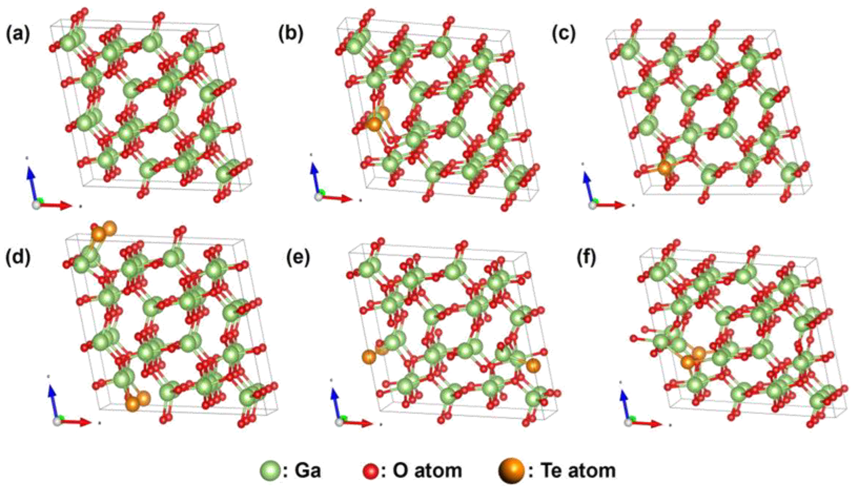
33]. Doping simulations employed an 80-atom
β-Ga₂O₃ supercell (a 1×2×2 expansion of the conventional 20-atom unit cell,
Figure 3a). In this supercell, Te doping replaced two Ga sites (%Te ~3.125%) or two O sites (%Te ~2.08%). Specifically, configurations involved substituting at two distinct Ga sites (GaⅠ, GaII) and three distinct O sites (OI, OII, OIII), as detailed in
Figure 2(b-f). The calculated total energies for these five configurations were -472.29068 eV, -472.92921 eV, -469.52646 eV, -468.05107 eV, and -468.71055 eV, respectively. Analysis revealed that the configuration with Te substituting at the OⅠ site, which had the lowest total energy, is thermodynamically preferred.
Formation energies in the neutral charge state were calculated for scenarios in which Te doping replaced three distinct oxygen sites (O
I, O
II, O
III) using methods from ref[
33]. Under O-rich (μ
O = 0) condition, formation energies for Te at OI, OII, and OIII sites were computed as -2.51 eV, -1.03 eV and -1.69 eV. Under O-poor (μ
Ga = 0) conditions, they are 2.47 eV, 3.94 eV and 3.28 eV, respectively. We found that the formation energy is lower under O-rich conditions, suggesting that Te is suitable for replacing O atoms in
β-Ga
2O
3 under these conditions. Notably, Te preferentially occupies O
I sites under both conditions due to the lowest formation energy (O
I < O
II < O
III).
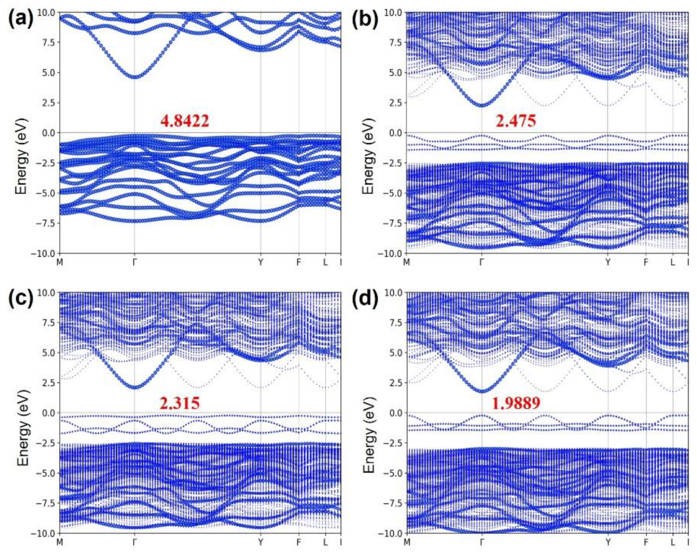
Figure 4(a) shows the effective band structures of
β-Ga₂O₃, it can be observed that the conduction band minimum (CBM) is positioned at the Γ-point, whereas the VBM is situated at the I-L line. The indirect energy bandgap of 4.8422 eV aligns well with the experimental values. As shown in
Figure 4(b)-(d), the bandgap of
β-Ga₂O₃ decreases when Te replaces different oxygen sites. Specifically, the bandgap is 2.475 eV when OI is replaced, 2.315 eV for O
II, and 1.989 eV for O
III. The VBM of Te-doped
β-Ga₂O₃ is lifted because of atomic orbitals, similar effect has been reported for anion doping using Se [
33,
34].
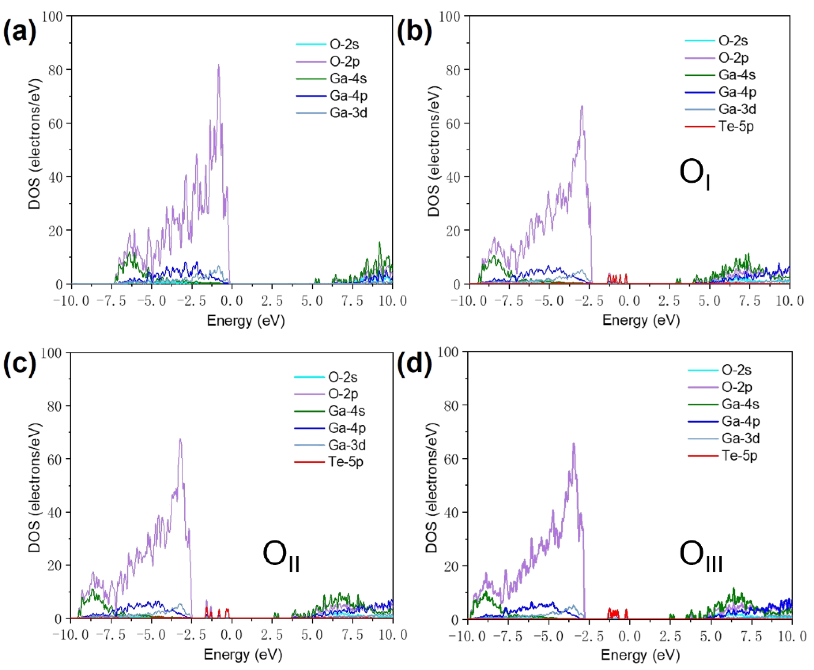
To explain in more detail how the band structure changed, we analyzed the density of states of Te-doped
β-Ga
2O
3. As depicted in
Figure 5(a), the projected density of states (PDOS) illustrates that the band edges of pure
β-Ga
2O
3 are dominated by O 2p and Ga 4s orbitals. The bandgap of
β-Ga
2O
3 is determined by the occupancy of VBM by O 2p orbital electrons and the CBM by Ga 4s orbital electrons.
Figure 5(b)-(d) shows the projected density of states of Te-doped
β-Ga2O3 at different oxygen sites. According to atomic orbital theory, the energy level of Te 5p is higher than that of O 2p, and the localization of the VBM composed of O 2p derived states is reduced, which is beneficial for improving hole mobility.
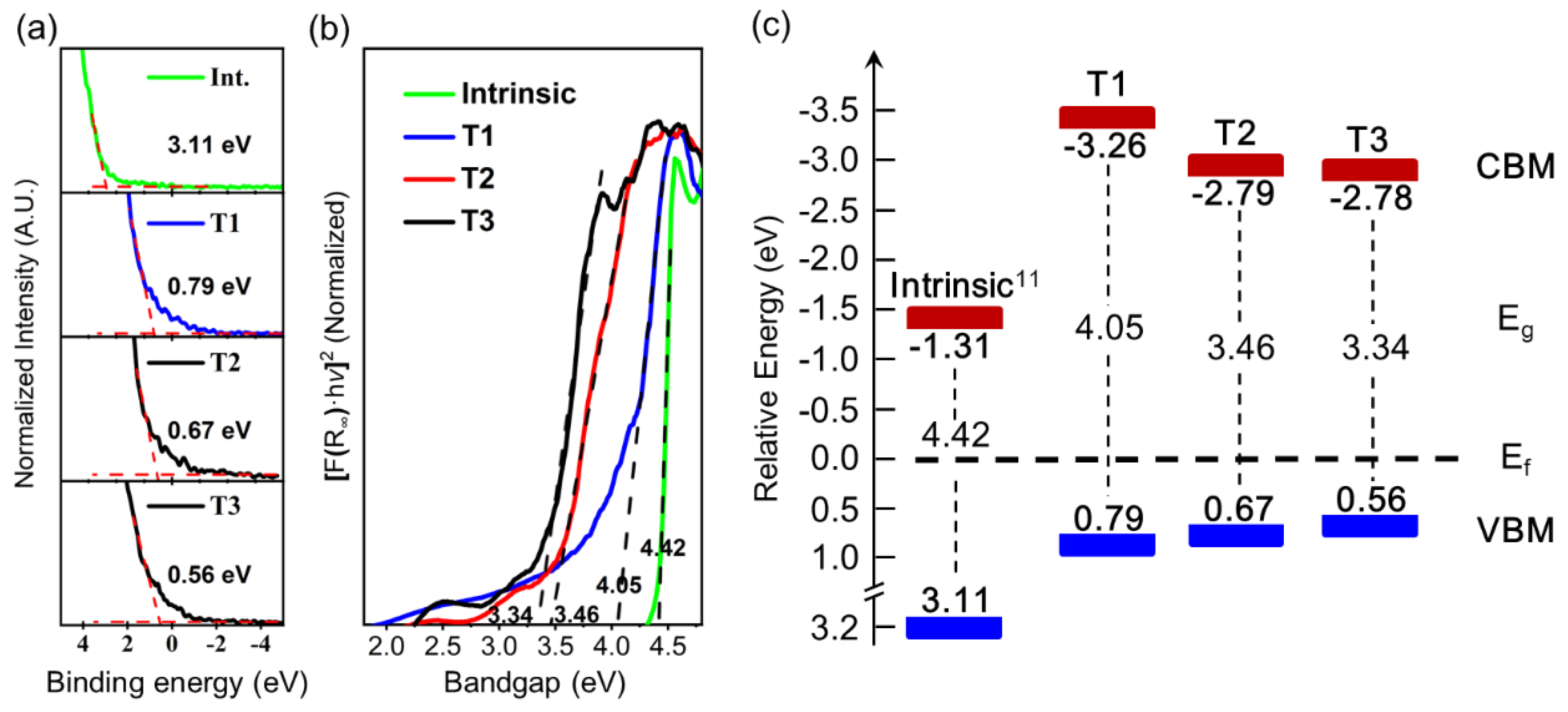
Figure 6(a) presents the VB-XPS results for Te-Mg co-doped
β-Ga₂O₃ samples (T1–T3), calibrated against a silver reference. The VB edge energy decreases from 0.79 eV (T1) to 0.67 eV (T2) and 0.56 eV (T3) with increasing Te content, which reduced about 2.5 eV from the intrinsic sample (3.11 eV), confirming p-type carrier dominance as the Fermi level shifts toward the VBM. Complementary optical bandgap narrowing is observed in
Figure 6(b), derived from Tauc plots using UV-Vis DRS. The bandgaps decreased from 4.42 eV (intrinsic) to 4.05 eV (T1), 3.46 eV (T2) and 3.34 eV (T3), paralleling the VB edge shift with Te doping. The optical bandgap measured in this study (4.05–3.34 eV, depending on Te content) is higher than simulated results for
β-Ga₂O₃ with ~2% Te incorporation, suggesting that the actual Te content in samples T1–T3 is below 2%.
By combining data acquired from VB-XPS and UV-Vis DRS into the schematic band structure (
Figure 7c), it reveals a systematic Fermi level migration in Te-Mg co-doped
β-Ga₂O₃. Compared to intrinsic
β-Ga₂O₃ [
11] measured in another word from our group, where the Fermi level resides closer to the conduction band minimum (CBM), indicative of n-type conductivity, the co-doped samples exhibit a pronounced shift of the Fermi level toward the VBM. This transition confirms a fundamental change in carrier type, transitioning from donor-dominated (n-type) to acceptor-dominated (p-type) conductivity.
However, some refinements are still needed for further developing this co-doping technique. For instance, to increase carrier concentration and reduce the resistivity to below 1 Ohm·cm [
35]. Besides, to better understanding the growth mechanism and carrier transport of the co-doping process is essential [
36].
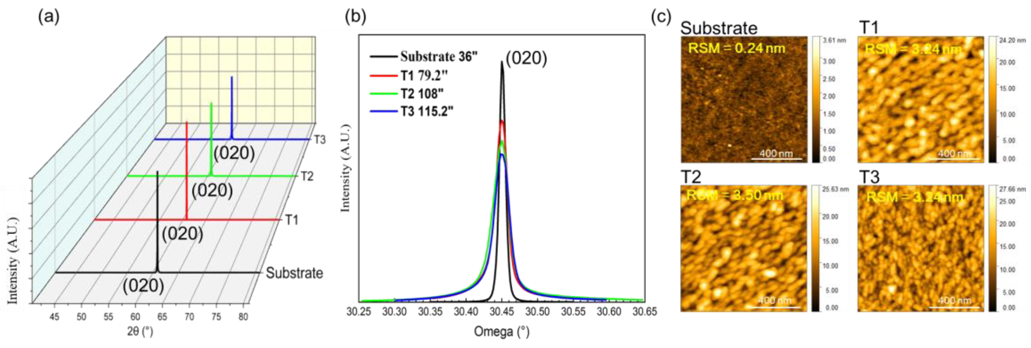
Figure 8(a) and 8(b) reveal the crystalline quality of the synthesized films characterized by X-ray diffraction (XRD).
Figure 8(a) shows that the p-type
β-Ga
2O
3 film grows epitaxially along (020) direction of the substrate, exhibiting single-orientation growth that maintains the single-crystal structure. The crystalline quality was quantified using the full width at half maximum (FWHM) of the XRD rocking curve.
Figure 8(b) shows the crystal quality of the film deteriorates from 79.2 arcsec to 115.2 arcsec, which indicated overall good crystal quality.
The change of structure and surface morphology before and after growth have been used for investigating using atomic force microscope (AFM), shown in
Figure 7. The overall roughness of the as-grown thin film is not small, potentially owing to the low growth temperature. As Te-doping increases, the grain size of the as-grown film becomes smaller, despite no obvious roughening, which demonstrates similar trends with what XRD rocking curves.