
Submitted:
30 September 2025
Posted:
01 October 2025
You are already at the latest version
Abstract
Lasers with external electrical modulation are widely used in optical systems, but the generation of well-defined pulses often suffers from distortions in duty cycle and top optical power at high frequencies. This work addresses this limitation by presenting an automated setup for optical pulse correction that combines standard instrumentation with a feedback-based adjustment strategy. The system integrates a continuous-wave laser, a signal generator, an optical analyzer, and a control routine implemented in MATLAB. Two nested loops are employed: the inner loop varies the amplitude of a sinusoidal modulation signal to regulate the duty cycle at the desired reference; the outer loop sends commands to the laser to adjust optical power level to a specified reference. Experimental validation shows that the proposed approach significantly improves pulse fidelity over a frequency range up to 100 MHz. In particular, the relative normalized root mean square error (NRMSE) was reduced by more than 97% compared with the case without adjustment, both for duty cycle (1–30 MHz) and top optical power (10–30 MHz). These results demonstrate that precise optical pulse control can be implemented with common laboratory instrumentation, providing a practical and accessible solution for automated pulse conditioning in externally modulated laser setups.
Keywords:
Externally modulated laser
; Laser diode modulation
; Optical pulse correction
; Top optical power
; Duty cycle stabilization
; Feedback control algorithm
; Optical Instrumentation
1. Introduction
Electrically modulated diode laser sources have found essential applications in nonlinear laser microscopies [1,2], in ultrahigh resolution (UHR) optical coherence tomography (OCT) [3,4,5], in ablation process (PLA) for particle size reduction in non-steroidal anti-inflammatory drugs (NSAIDs) [6], as a trigger source in sampling circuits for photonics and optoelectronics analog to digital converters [7,8,9], among others. To improve the performance in these applications, it is relevant to have a high quality light source, in which the degradation of the optical pulse repetition rate (OPPR), duty cycle and output power can be minimized for optimal operation. To electrically modulate a laser diode two approaches can be used: external modulation that use electro-optic or acousto-optic modulators, which provides high bandwidth and low chirp but at the expense of complexity and cost; and direct modulation, where the electrical signal is applied to the laser diode itself, which simplifies the system but introduces limitations in distortion and stability [10,11]. Similarly, different methods have been proposed to improve OPRR and duty cycle. For example, methods based on Fourier transforms and spatial light modulators allow almost arbitrary shaping of optical pulses on the order of femtoseconds , while waveguide array (AWG) synthesizers and frequency combs have demonstrated pulse trains of up to 10 GHz with phase and amplitude control [12]. Other approaches use fiber Bragg gratings with forward correction algorithms, achieving higher conversion efficiencies than previously reported [13], or Mamyshev-type regenerative configurations capable of generating eigenpulses with stable parameters after multiple cycles [14]. At the gain dynamics level, it has recently been shown that quasi-synchronous pump modulation in Er- and Yb-doped fibers can induce high-energy pulse trains with great stability [15].
Due to recent technologies, such as AI and G8, that reveal a future of high technological demands there is a growing need for optical pulses with high temporal quality, both in their pulse width and in the flatness and stability of their upper level. This requirement is critical when pulses are used to trigger optoelectronic switches, drive high-speed modulators, or control sensitive nonlinear devices. In such scenarios, small distortions in the electrical modulation signal can translate into significant variations in the optical pulse quality that can seriously compromise applications performance. Recent studies have highlighted how temporal quality of pulses allows for the optimization of fast physical interactions [16], and how spatiotemporal manipulation pulse sequences enables customizable top-hat profiles useful in ultrafast switching applications [17,18]. However, most studies focus on complex optical techniques, while little is reported on how actual electrical conditions—50 Ω impedances, resistive attenuation dividers, and parasitic capacitances of laser ports and measurement equipment—affect the shape and amplitude of optical pulses when using commercial CW modules with external modulation input. This aspect is crucial because, according to application notes and works on direct modulation, even simple mismatches can excite relaxation resonances and produce significant sideband power [10,19], causing discrepancies between the signal measured on the oscilloscope and the one actually applied to the laser.
This work presents an automated feedback measurement setup for optical pulse correction that combines standard instrumentation with a feedback-based adjustment strategy. The setup provides the characterization of external electrical modulation signals applied to the continuous wave diode laser and its effect on the temporal form of the optical signal. An equivalent circuit of the resistive-capacitive network formed by the generator, the attenuators, and the 50 Ω loads of the trigger and measurement ports is presented, in order to interpret the experimentally observed trends. Amplitude measurements of the laser trigger signal versus frequency (10 kHz–100 MHz) show how the measurement node exhibits band-pass behavior, while the laser trigger port exhibits a low-pass filter-like effect. This analysis highlights the importance of considering the electrical and instrumental setup when interpreting results. The findings complement advances in optical pulse correction and direct diode modulation, offering practical insights for scientists and engineers working with commercial lasers who need to understand the real-world limitations of electrical excitation.
2. Materials and Methods
2.1. Practical Implementation
Figure 1 shows a block diagram of the implemented measurement and control system layout, which includes an Obis LX 660 coherent laser, a Tektronix AFG3101 signal generator, and an HP8340A network analyzer. The laser is connected to an optical channel of the analyzer (red line) via optical fiber and a 1x2 optical splitter with an aspect ratio of 95:5. The generator provides the electrical signal that activates the laser pulses, this signal is measured by an electrical channel of the analyzer through an attenuating SMT resistor, in addition this signal is used as a trigger for the electrical channel of the analyzer (yellow line). All instruments are connected to a computer programmed to control their individual and combined operation (purple line). The laser and generator receive commands to adjust their parameters, and the analyzer sends information to the PC to establish the feedback control system.
Figure 2 shows an equivalent electrical diagram of the connected instruments. represents the internal resistance of the generator output port, the input resistance of the laser trigger port, the resistor on a surface mount plate used to attenuate 10x the analyzer electrical channel, and the input resistance of the electrical channel and the analyzer trigger respectively. , , and represent the capacitance of the generator port, the laser trigger port, the surface mount plate, the electrical channel of the Analyzer and the trigger channel, respectively. In the circuit shown in Figure 2, the signal at behaves as a low-pass filter because of the resistive-capacitive circuit formed between and . At low frequencies, the capacitor behaves as an open circuit and allows the signal to pass, while at high frequencies it becomes conductive and diverts the signal to ground, reducing the gain.
On the other hand, the signal at presents a band-pass behavior, since it is located between two independent low-pass R-C structures, which attenuate both low and high frequencies but allow maximum transmission in an intermediate band, producing maximum gain at a certain resonant frequency. Therefore, as the frequency of the laser trigger electrical signal increases, its amplitude will be reduced, which affects the duty cycle of the optical pulses. For this reason, it is necessary to apply amplitude compensation to the electrical signal, which is achieved in this work by automating the measuring and signal generation instruments.
2.2. Laser Activation with Pulsed Electrical Signal
The OBIS LX660 system includes a continuous wave (CW) laser diode that can be modulated with an external electrical signal via an internal driver circuit. For optical pulse generation in digital modulation mode, it requires a signal equal to or greater than 1.5 V to be activated and a signal less than 1 V to be deactivated. Figure 3 and Figure 4 show for 10 KHz and 30 MHz the electrical activation signal and the obtained modulated optical signal. The used pulsed trigger had a 20% duty cycle with an amplitude of 2 V peak-to-peak and an offset of 1 V. For both cases (10 kHz and 30 MHz), the laser was set at 50 mW of optical power. In Figure 4 it is observed that the top optical power is around 40 mW and its duty cycle is around 15%, where both values decreased with respect to Figure 3. In addition, the waveform of the electrical signal has been deformed, this is due to the frequency response of the electrical signal explained above. The proposed automated feedback measurement setup mitigates these effects. (The top optical power level refers to the upper amplitude of the pulse and is calculated as the average of the most common and stable levels in the distribution of amplitudes obtained by a histogram function.)
2.3. Laser Activation with Sinusoidal Electrical Signal
In this work a sinusoidal electrical signal is used to modulate the laser, as electrical signal generators can produce it at higher frequencies compared to the square signal (i.e., the AFG3101 generator can produce a sinusoidal signal up to 100 MHz, while the square signal is only generated up to 50 MHz for a 30% duty cycle).
Figure 5 shows a sinusoidal signal, the continuous horizontal line is the On threshold of laser activation and the dotted line is the Off threshold, the sinusoid has a peak-peak amplitude of 1.5 V and an offset of 0.75 V, with these values a duty cycle of 19.59% is calculated for the optical pulses, that is, depending on the portion of the sinusoid that reaches the on and off threshold, the laser will be activated with a certain duty cycle, the equations used to calculate this are explained below.
In equations 1 and 2, On is the turn-on threshold, Off is the turn-off threshold, is the peak-peak value of the sinusoid, is the period of the sinusoid, is the time at which the sinusoid becomes equal to On and is the time after at which the sinusoid becomes equal to Off. By solving and and substituting in equation 3, the value of that achieves a certain duty-cycle is obtained. Table 1 presents calculated values that show how increasing increases the duty cycle even though the offset value remains constant.
Figure 6 shows a 10 kHz sinusoidal electrical signal used to modulate the laser and the modulated obtained optical pulses. The sinusoidal electrical signal has amplitude = 0.98 V and offset = 0.865 V. The duty cycle of the optical pulses is 19.78%. This measured value is close to that calculated with the equations already mentioned, it should be noted that the value measured from the electrical channel is attenuated about 21 times with respect to the value that reaches the laser trigger by the effects of resistive dividers mentioned in the measurement circuit. In addition, will decrease as the frequency increases due to the low-pass filter effect already mentioned, so that it is necessary for each required frequency to adjust the to achieve a certain desired duty cycle.
Figure 7 shows a 100 MHz sinusoidal electrical signal used to modulate the laser and the modulated obtained optical pulses. An Opp = 14.436 V and offset of 0.865 V were established in the sinusoidal signal by the feedback adjustment algorithm. From the figure optical pulses are generated with top power value of 50.8 mW and duty cycle of 19.2%. It is observed that the resulting pulses have some overshoot, and their waveform is not square, this is due to inherent limitations in the laser response, even so, they are close to the reference values of top optical power 50 mW and duty cycle of 20%.
2.4. Feedback Adjustment Algorithm
To implement the algorithm for adjusting the duty cycle and the top optical power of the laser pulses a Matlab program was developed, the program automates the operation of the laser, generator, and analyzer. The general procedure is shown in Figure 8 with a flowchart. The initial step consists of defining the desired values for duty cycle, optical power, and frequency set for the optical pulses. In the generator, the output impedance, sine waveform, offset, initial frequency, and initial are configured. In the laser, the optical power is adjusted, and the constant beam mode is activated, next, a routine is applied to the analyzer to measure the power level, this level will later be used as a reference for the optical pulse power adjustment loop. Afterwards, a for loop is executed in which for each iteration each frequency value is adjusted in the generator and the time base is adjusted in the analyzer, then the duty cycle adjustment loop is applied, the current duty cycle is measured using a routine in the analyzer and the of the laser trigger signal is adjusted iteratively until the measured duty cycle matches the reference duty cycle within a defined tolerance. The optical power adjustment loop is then applied, where the top power level is measured and the laser is iteratively adjusted until the measured power matches the reference power. At the end of the for loop, all the data measured by the analyzer is saved.
Figure 9 a) shows a flowchart of the duty cycle adjustment loop, where the of the sinusoidal signal that activates the laser is adjusted to reach the reference duty cycle. To do this, an iterative process is used that measures the current duty cycle and calculates the difference with respect to the reference duty cycle, denoted as difD. To measure the signals, a routine called Niv is executed (Figure 9 c)), which measures the waveform of the optical laser signal and the electrical activation signal. The procedure begins by measuring the duty cycle of the optical signal and calculating the difference between the reference value and the measured value. If this difference is within an acceptable tolerance (tolD), the algorithm concludes. Otherwise, an assessment is made as to whether the measured average power Pmed is less than 50% of the reference power (PotRef). If so, is increased by 100 mV, the power is measured again, and the difference difD is recalculated.
When the measured average power is greater than 50% of the reference, but the duty cycle is still not adequately adjusted, more precise modifications to are applied depending on both the sign and magnitude of difD. If the measured duty cycle is less than the reference, and the difD error is greater than 5%, is increased by 100 mV. If difD is between 2% and 5%, is increased by 50mV, and if it is less than or equal to 2%, is increased by 5mV. On the other hand, if the measured duty cycle is greater than desired, reductions are applied following a similar logic: if difD is less than -5%, is reduced by 100mV; if it is between -5% and -2%, it is reduced by 50mV; and if it is greater than or equal to -2%, the reduction is 5mV.
After each adjustment, the algorithm measures again the duty cycle and recalculates difD, repeating the cycle until the error is reduced to a value within the established tolerance. This procedure implements rule-based control that allows for progressive and efficient convergence, using variable adjustment steps depending on the magnitude of the error. In the optical power adjustment loop (Figure 9 b)), the top power of the pulses is first measured, and the difference between the measured and reference power is calculated. If the difference exceeds the defined tolerance and the measured power is lower than the reference power, a 0.5 mW increment is applied to the laser; if the measured power exceeds the reference power, a 0.5 mW decrement is applied. This is repeated until the measured optical power value approaches the reference value, i.e., until the difference is within the tolerance.
3. Results
Figure 10 shows the top optical power measurements versus frequency values without applying the adjustment algorithm (line with an asterisk) and with the adjustment algorithm (line with a circle) for a reference power of 50 mW. The figure shows that, without the adjustment algorithm, the maximum optical power decreases as the frequency increases. On the other hand, with the algorithm, the top optical power remains close to the reference as the frequency increases. To evaluate the performance of the adjustment algorithm, the Normalized Root Mean Square Error (NRMSE) was calculated for all measured top power values with respect to the reference power. With the algorithm, the NRMSE is 0.98%; without the algorithm, the error is 8.41%, that is, almost an order of magnitude larger, the relative NRMSE decreased by 88.3% when applying the algorithm. Furthermore, the difference becomes more noticeable at frequencies between 10 MHz and 30 MHz, where the NRMSE was 18.5% without the algorithm, while with the proposed algorithm it was reduced to 0.49%, equivalent to a relative improvement of 97.3%. This result shows that the algorithm manages to maintain the optical power practically at the reference value (50 mW), with specific deviations less than 1%.
In Figure 11 the measured values of duty cycle vs the frequency are observed for a reference duty cycle of 20%, the line with asterisks represents the measurements without applying the algorithm, in which from frequencies greater than 1 MHz, the duty cycle decreases to a value around 12% at 20 MHz, while the line with circles corresponds to the measurements when applying the adjustment algorithm, it can be seen that the duty cycle remains very close to 20% for all frequency values up to 100 MHz. It should be noted that in the measurements without applying the algorithm in both Figure 10 and Figure 11 the frequency values reach up to 30 MHz because a pulse signal cannot be generated at a duty cycle of 20% with higher frequencies with the generator used, on the other hand the measurements when applying the algorithm in both figures reach up to 100 MHz since the activation sinusoidal signal can be generated up to this frequency.
The NRMSE was calculated for all measured duty cycle values with respect to the reference duty cycle; with the adjustment algorithm, the NRMSE was 0.472%; without the algorithm, the error was 5.695%; the relative NRMSE decreased by 91.7% when applying the algorithm. At frequencies between 1 MHz and 30 MHz, the NRMSE was 21.1% without the algorithm, while with the proposed algorithm it was reduced to 0.6%, which is equivalent to a relative improvement of 97.13%.
In Figure 12 the measured values of top optical power vs. frequency are shown for a reference power of 40 mW, similarly to Figure 10, for frequencies between 10 MHz and 30 MHz the top optical power decreases considerably without the adjustment algorithm (line with asterisks), while when applying the algorithm (line with circles) the top power values are kept very close to the reference. In Figure 13 the measured values of duty cycle vs. frequency are shown for a reference duty cycle of 30%, similarly to Figure 11, for frequencies between 1 MHz and 30 MHz it is observed the decrease in the measured duty cycle without applying the algorithm (line with asterisks) while when applying the algorithm (line with circles) the measured duty cycle remains very close to the reference duty.
Table 2 summarizes the NRSME error values calculated from the top optical power measurements with and without applying the adjustment algorithm, considering the frequency values from 10 to 30 MHz for both cases shown in Figure 10 and Figure 12, that is, with a reference power of 50 mW and another of 40 mW, it is noted that the relative improvement in both cases is greater than 95% when applying the algorithm.
Table 3 summarizes the NRSME error values calculated from the duty cycle measurements with and without applying the adjustment algorithm, for the frequency values from 1 MHz to 30 MHz for both cases shown in Figure 11 and Figure 13, that is, with a reference duty cycle of 20% and another of 30%, the relative improvement in both cases is greater than 95% when applying the algorithm.
4. Discussion
The presented automated setup and closed-loop control strategy for optical pulse correction allow external modulation of the laser to adjust the duty cycle and top optical power over a wide frequency range. Obtained results confirm the effectiveness of the proposed algorithms and control scheme. Without applying the algorithm, a significant degradation of both metrics is observed as the frequency increases. Applying the proposed algorithm, deviations from the reference values are reduced to sub-percentage values, with relative improvements exceeding 95% in all evaluated cases. The use of sinusoidal excitation as modulator signal allowed extending the control up to 100 MHz, overcoming the practical limitation of the generator in pulse mode for low duty cycles. For top optical power, in the 10-30 MHz range, the obtained normalized root mean square error (NRMSE) applying algorithm was almost two orders of magnitude lower than without applying it, representing a relative improvement of over 97% compared to not using the adjustment. Similarly, for the duty cycle in the 1-30 MHz range, the NRMSE decreased to sub-percentage values, also equivalent to a relative reduction of over 97% compared to the condition without the algorithm. This trend was consistently observed in both test sets, with references of 50 mW top power and 20% duty cycle and 40 mW top power and 30% duty cycle, demonstrating that the method not only stabilizes the pulses but also provides a clear quantitative improvement compared to the uncorrected case.
Although pulses exhibit some overshoot and distortion at frequencies close to 100 MHz, these correspond to the inherent limitations of the laser and cannot be eliminated with this type of control. However, the proposed approach shows that self-tuning can be implemented without the need for highly specialized instrumentation. In fact, although a high-performance analyzer was used in this work, the same procedure could be reproduced with more common laboratory instruments, such as an oscilloscope equipped with an integrated photodiode probe for detecting optical pulses. This highlights the versatility of the method and its potential for application in more accessible experimental settings. The findings are consistent with literature reports on the limitations of direct modulation of laser diodes and commercial modules with electrically modulated inputs. Previous studies show that, as the modulation frequency increases, the interaction between the generator output impedance, the internal resistances of the measurement and trigger ports, and the parasitic capacitances produces a combined low-pass and band-pass filter behavior that distorts the pulse shape [10,11,19].
The relevance of correction realized with the proposed algorithms and control scheme becomes evident when considering the need for high temporal quality optical pulses in optoelectronic applications. As reported in optical interconnects [20], photoconductive switches [21] and ultrafast photodiode-based samplers [22], small distortions in the pulse time profile can affect the triggering efficiency, linearity or fidelity in the reconstruction of analog signals. In this context, the ability to maintain both the top power and the duty cycle within sub-percentage margins in the face of frequency variations represents a practical step towards more robust and predictable systems.
Overall, the discussion of the results demonstrates that the presented strategy not only addresses the immediate limitations of available hardware (commercial generators and modules) but also opens the possibility of extending automatic control techniques to more accessible laboratory settings, where high-end instrumentation is not always available.
Author Contributions
“Conceptualization, I.O.H.-F., C.V.-A and D.O.B.-N; methodology, I.O.H.-F., C.V.-A and D.O.B.-N; software, I.O.H.-F and D.O.B.-N; validation, I.O.H.-F and D.O.B.-N.; formal analysis, I.O.H.-F, C.V.-A, D.O.B.-N and R.M.-C.; investigation, I.O.H.-F, C.V.-A, D.O.B.-N, R.M.-C. and R.V.-A; writing—original draft preparation, I.O.H.-F and C.V.-AA; writing—review and editing, D.O.B.-N, R.M.-C, R.V.-A;. All authors have read and agreed to the published version of the manuscript.”
Funding
“This research received no external funding”.
Institutional Review Board Statement
Not applicable
Informed Consent Statement
Not applicable
Data Availability Statement
The main data are provided in the article. Any other raw/processed data required to reproduce the findings of this study are available from the corresponding autor upon request.
Acknowledgments
The authors are grateful to the The Secretariat of Science, Humanities, Technology and Innovation of Mexico (SECIHTI) for supporting a scholarship for the doctoral studies of Daniel Omar Baez-Nuñez.
Conflicts of Interest
The authors declare no conflicts of interest.
References
- Ozeki, Y.; Umemura, W.; Otsuka, Y.; Satoh, S.; Hashimoto, H.; Sumimura, K.; Nishizawa, N.; Fukui, K.; Itoh, K. High-speed molecular spectral imaging of tissue with stimulated Raman scattering. Nat. Photonics 2012, 6, 845–851. [CrossRef]
- Xu, C.; Wise, F.W. Recent advances in fiber lasers for nonlinear microscopy. Nat. Photonics 2013, 7, 875–882. [CrossRef]
- Nishizawa, N.; Chen, Y.; Hsiung, P.; Ippen, E.P.; Fujimoto, J.G. Real-time, ultrahigh-resolution optical coherence tomography with an all-fiber, femtosecond fiber laser continuum at 1.5 μm. Opt. Lett. 2004, 29, 2846–2848. [CrossRef]
- Aguirre, A.D.; Nishizawa, N.; Seitz, W.; Lederer, M.; Kopf, D.; Fujimoto, J.G. Continuum generation in a novel photonic crystal fiber for ultrahigh-resolution optical coherence tomography at 800 nm and 1300 nm. Opt. Express 2006, 14, 1145–1160. [CrossRef]
- Nishiura, M.; Kobayashi, T.; Adachi, M.; Nakanishi, J.; Ueno, T.; Itoh, Y.; Nishizawa, N. In vivo ultrahigh-resolution ophthalmic optical coherence tomography using Gaussian-shaped supercontinuum. Jpn. J. Appl. Phys. 2010, 49, 012701. [CrossRef]
- Gera, T.; Nagy, E.; Smausz, T.; et al. Application of pulsed laser ablation (PLA) for the size reduction of non-steroidal anti-inflammatory drugs (NSAIDs). Sci. Rep. 2020, 10, 15806. [CrossRef]
- Mohammadi, M.; Habibi, F.; Seifouri, M.; et al. Recent advances on all-optical photonic crystal analog-to-digital converter (ADC). Opt. Quant. Electron. 2022, 54, 192. [CrossRef]
- Villa-Angulo, C.; Hernández-Fuentes, I.O.; Morales-Carbajal, R.; Villa-Angulo, R.; Villa-Angulo, J.R. Characterization of a high-speed radio-frequency sampling and demultiplexing circuit based on the cascade connection of pin photodiodes. Turk. J. Electr. Eng. Comput. Sci. 2019, 27, 939–949. [CrossRef]
- Hernández-Fuentes, I.O.; Villa-Angulo, C.; Villa-Angulo, R.; Donkor, E. Linear operation range for an optically triggered switch based on a p-i-n photodiode. IEEE Photonics Technol. Lett. 2014, 26, 1813–1816. [CrossRef]
- Melentiev, P.N.; Subbotin, M.V.; Balykin, V.I. Simple and effective modulation of diode lasers. Laser Phys. 2001, 11, 891–896.
- Preuschoff, T.; Baus, P.; Schlosser, M.; Birkl, G. Wideband current modulation of diode lasers for frequency stabilization. Rev. Sci. Instrum. 2022, 93, 063002. [CrossRef]
- Weiner, A.M. Ultrafast optical pulse shaping: A tutorial review. Opt. Commun. 2011, 284, 3669–3692. [CrossRef]
- Parmigiani, F.; Oxenløwe, L.K.; Galili, M.; Ibsen, M.; Zibar, D.; Petropoulos, P.; Richardson, D.J.; Clausen, A.T.; Jeppesen, P. All-optical 160-Gbit/s retiming system using fiber grating based pulse shaping technology. J. Lightwave Technol. 2009, 27, 213–221. [CrossRef]
- Regelskis, K.; Liaugminas, G.; Želudevičius, J. Regenerative shaper of ultrashort light pulses. Photonics 2023, 10, 836. [CrossRef]
- Nyushkov, B.; Ivanenko, A.; Koliada, N.; Smirnov, S. Stationary high-energy pulse generation in Er-based fiber lasers via quasi-synchronous gain modulation. Photonics 2024, 11, 37. [CrossRef]
- Kim, J.H.; Choi, H.W. Review on principal and applications of temporal and spatial beam shaping for ultrafast pulsed laser. Photonics 2024, 11, 1140. [CrossRef]
- Xu, S.; Chen, Y.; Xia, R.; Duan, C.; Hu, X.; Zeng, Q.; Zhou, H.; Xiao, Y.; Tang, X.; Xu, G. Spatial-temporal manipulations of visible nanosecond sub-pulse sequences in an actively Q-switched Pr3+:YLF laser. Opt. Laser Technol. 2025, 183, 112247. [CrossRef]
- Zhu, X.; Li, C.; Guo, H.; Shi, X.; Sun, J.; Zhao, J.; Sun, H.; Wei, Y.; Zhang, X.; Wei, Z.; et al. Spatiotemporal shaping of high-power laser pulses based on Brillouin beam smoothing. Front. Phys. 2023, 10, 1110683.
- Wu, Y.; Liu, W.; Sun, X.; Chen, J.; Cheng, G.; Chen, X.; Fu, Y.; Liu, P.; Zhang, T. A Load-Adaptive Driving Method for a Quasi-Continuous-Wave Laser Diode. Micromachines 2024, 15, 355. [CrossRef]
- Keeler, G.A.; Nelson, B.E.; Agarwal, D.; Debaes, C.; Helman, N.C.; Bhatnagar, A.; Miller, D.A.B. The benefits of ultrashort optical pulses in optically interconnected systems. IEEE J. Sel. Top. Quantum Electron. 2003, 9, 477–485. [CrossRef]
- Keil, U.D.F.; Dykaar, D.R. Ultrafast pulse generation in photoconductive switches. IEEE J. Quantum Electron. 1996, 32, 1664–1671. [CrossRef]
- Clement, T.S.; Hale, P.D.; Williams, D.F.; Wang, C.M.; Dienstfrey, A.; Keenan, D.A. Calibration of sampling oscilloscopes with high-speed photodiodes. IEEE Trans. Microw. Theory Tech. 2006, 54, 3173–3181. [CrossRef]
Figure 1.
Block diagram of the implemented automated feedback measurement setup.
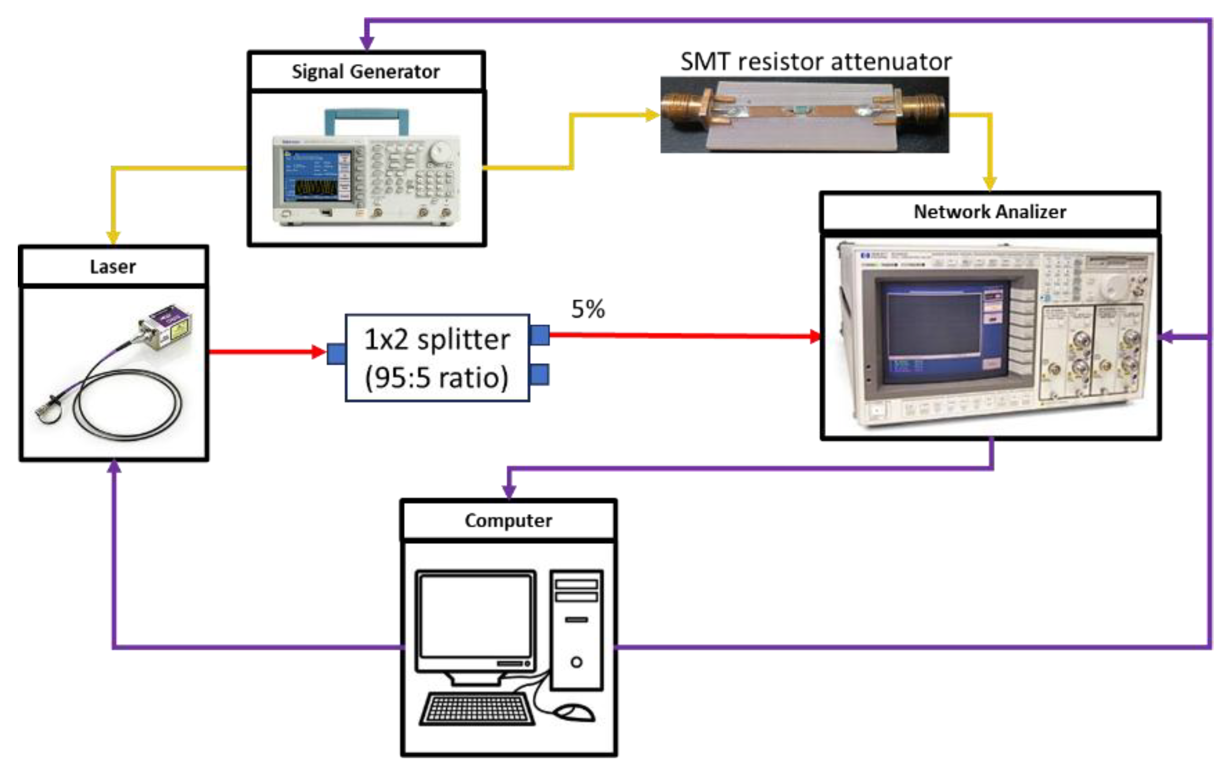
Figure 2.
Block diagram of the implemented automated feedback measurement setup.
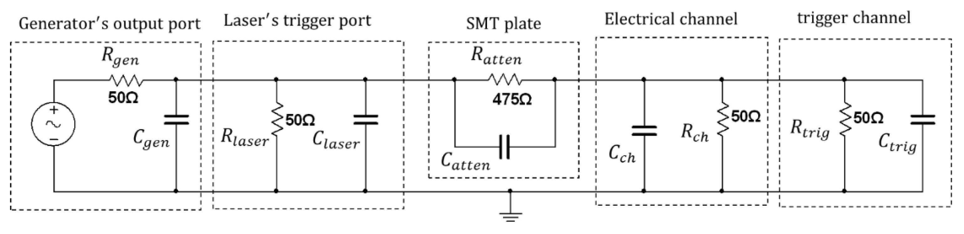
Figure 3.
Electrical pulse d signal at 10 kHz and resulting optical pulses without applying the feedback adjustment algorithm.
Figure 3.
Electrical pulse d signal at 10 kHz and resulting optical pulses without applying the feedback adjustment algorithm.
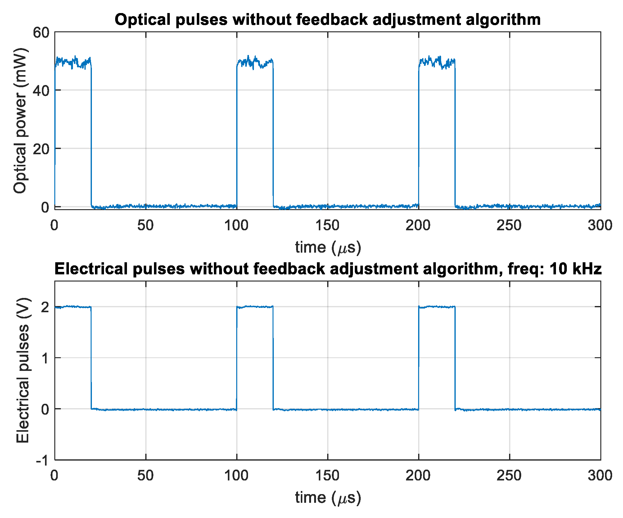
Figure 4.
Electrical sinusoidal signal at 10 kHz and resulting optical pulses, applying the feedback adjustment algorithm.
Figure 4.
Electrical sinusoidal signal at 10 kHz and resulting optical pulses, applying the feedback adjustment algorithm.
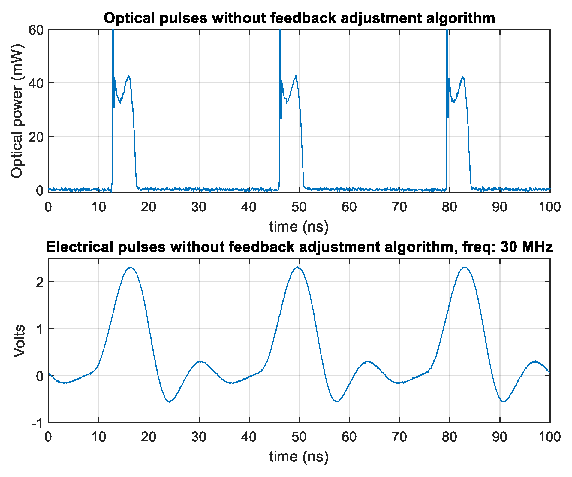
Figure 5.
Sinusoidal signal and on/off thresholds for laser triggering.
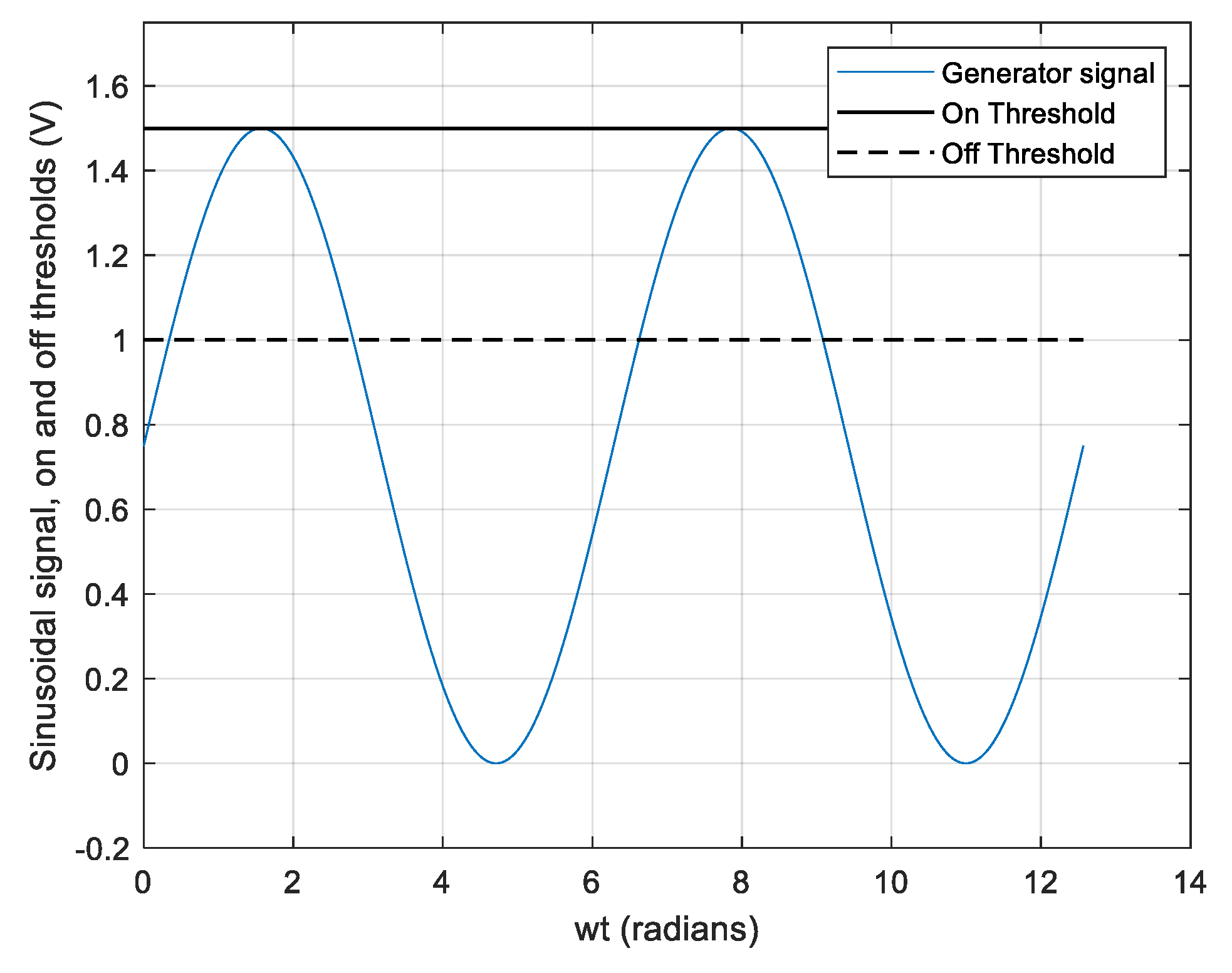
Figure 6.
Sinusoidal signal at 10 kHz and resulting optical pulses, applying the feedback adjustment algorithm.
Figure 6.
Sinusoidal signal at 10 kHz and resulting optical pulses, applying the feedback adjustment algorithm.
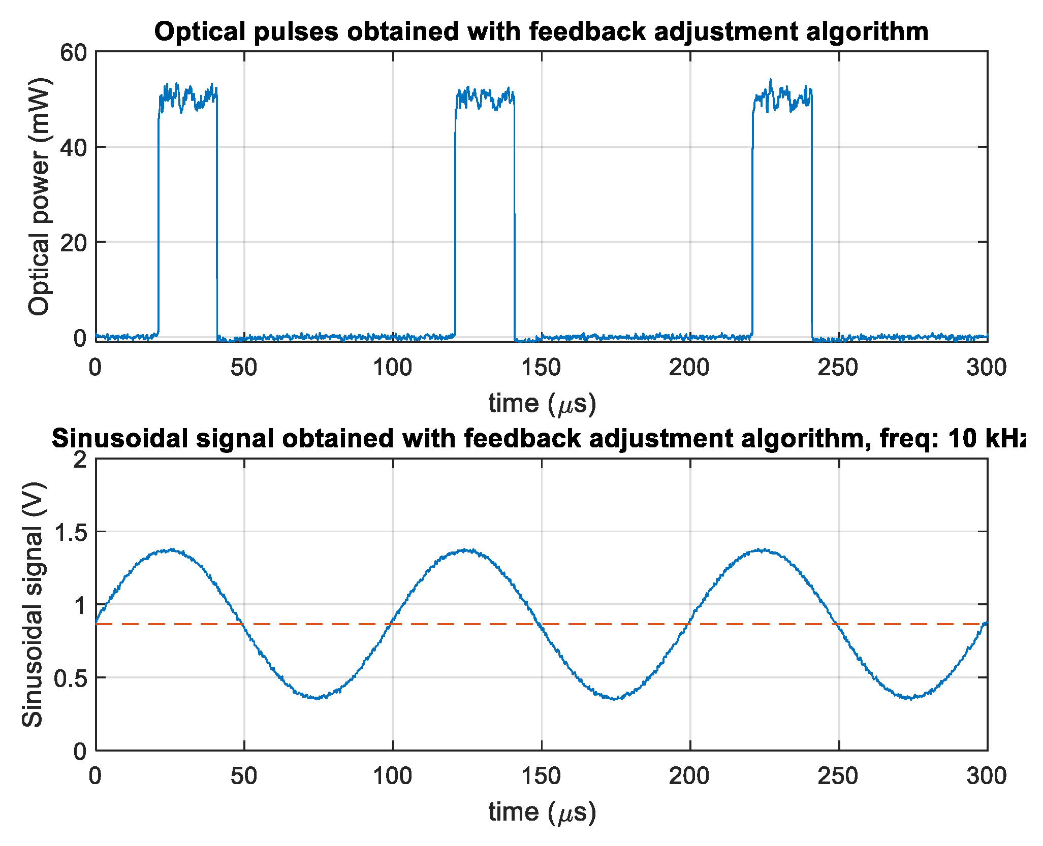
Figure 7.
Sinusoidal signal at 100 MHz and resulting optical pulses, applying the feedback adjustment algorithm.
Figure 7.
Sinusoidal signal at 100 MHz and resulting optical pulses, applying the feedback adjustment algorithm.
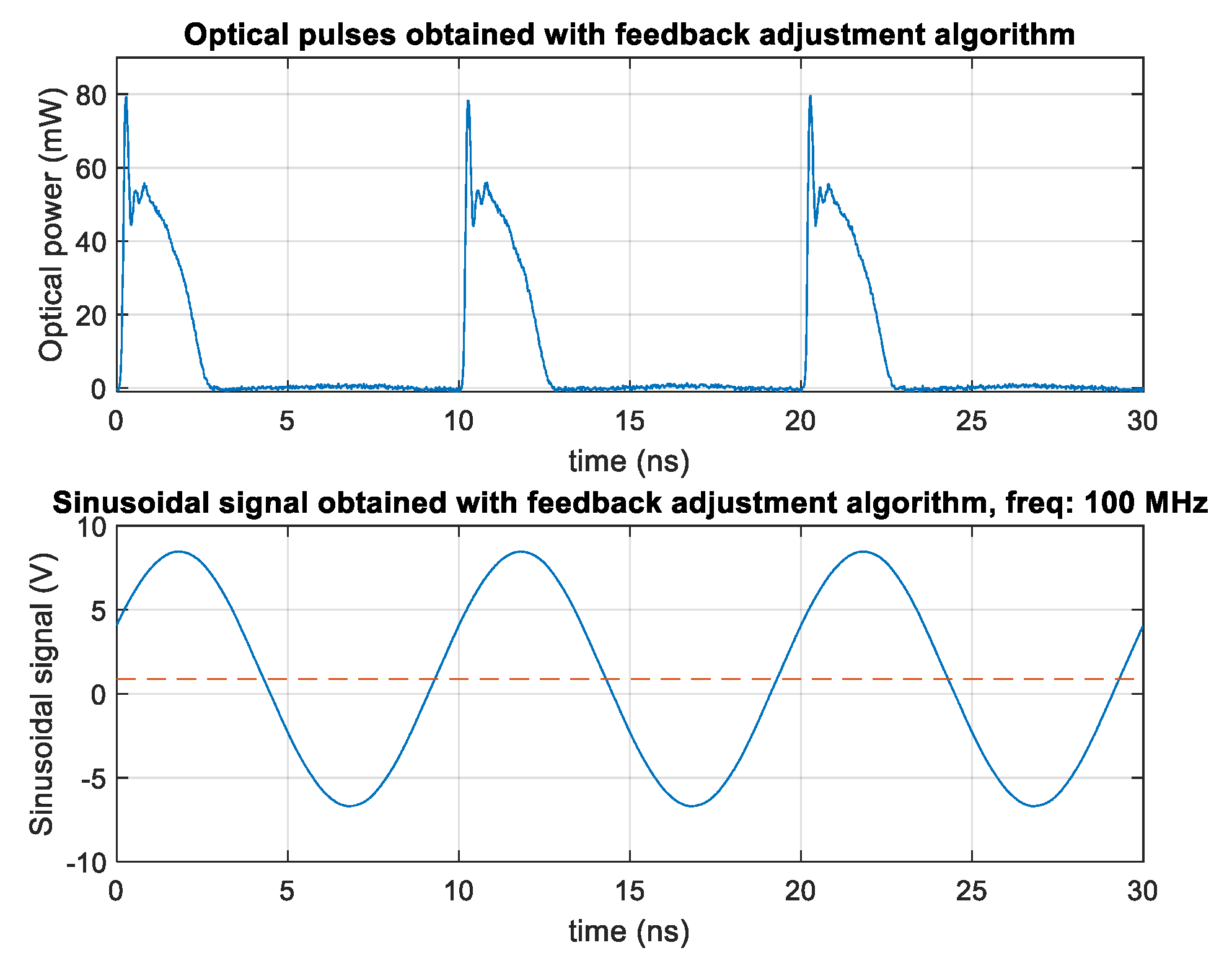
Figure 8.
Main loop of the algorithm for adjusting the optical pulses of the laser.
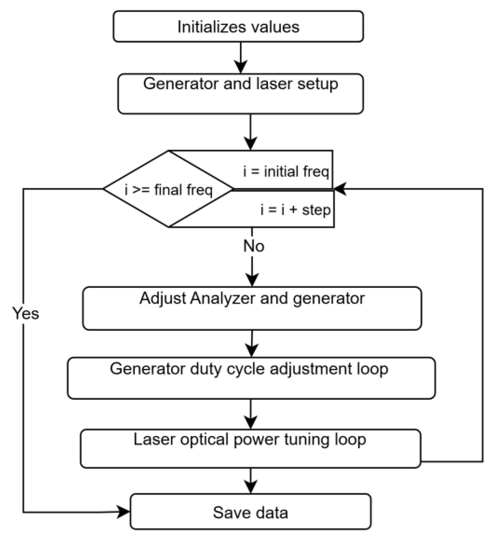
Figure 9.
Flowcharts: a) duty cycle adjustment algorithm, b) optical power adjustment algorithm and c) measurement routine.
Figure 9.
Flowcharts: a) duty cycle adjustment algorithm, b) optical power adjustment algorithm and c) measurement routine.
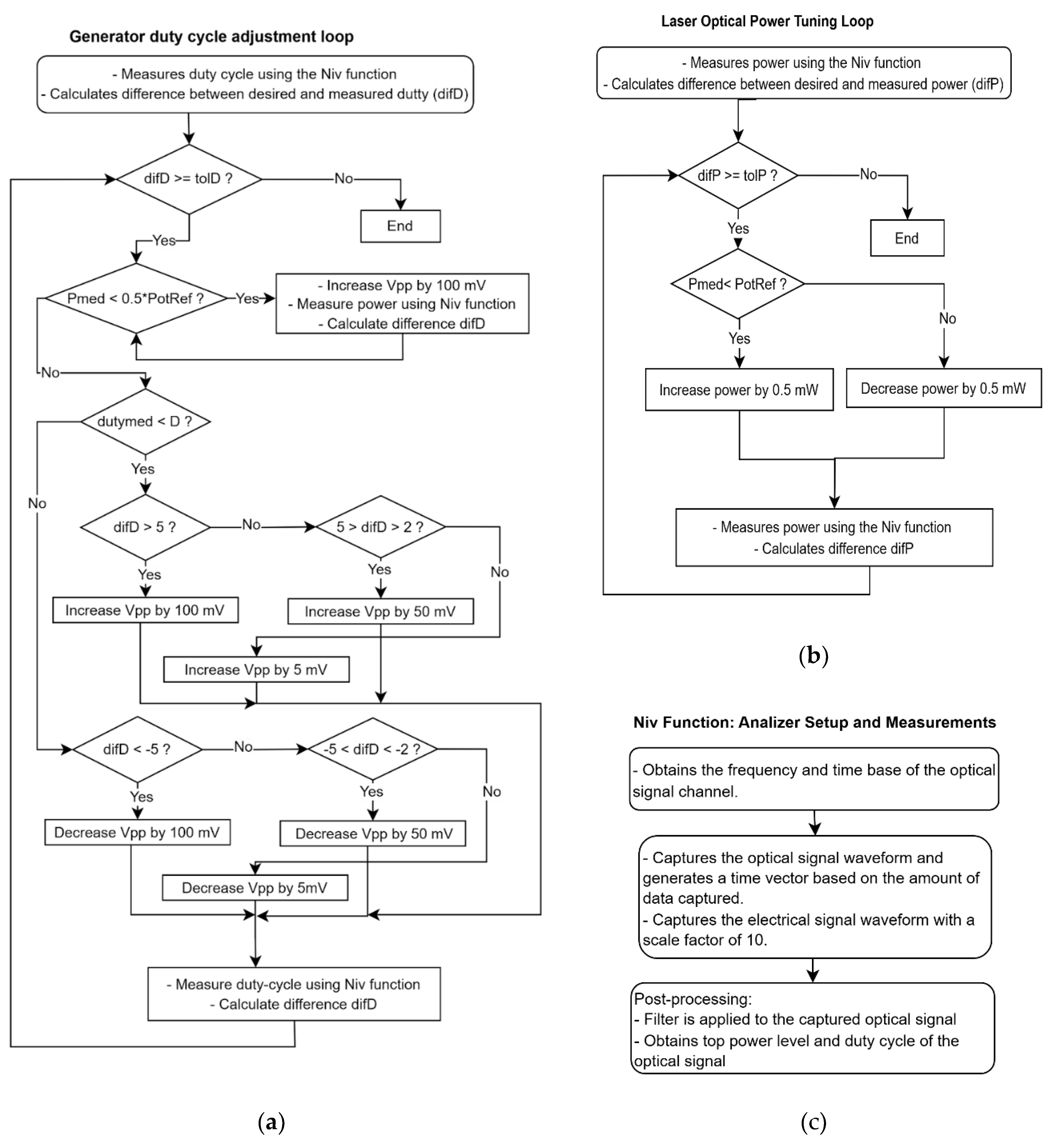
Figure 10.
Top optical power vs frequency applying the adjustment (circled line) and without applying the adjustment (asterisked line). (Potref = 50 mW, duty cycle =20%).
Figure 10.
Top optical power vs frequency applying the adjustment (circled line) and without applying the adjustment (asterisked line). (Potref = 50 mW, duty cycle =20%).
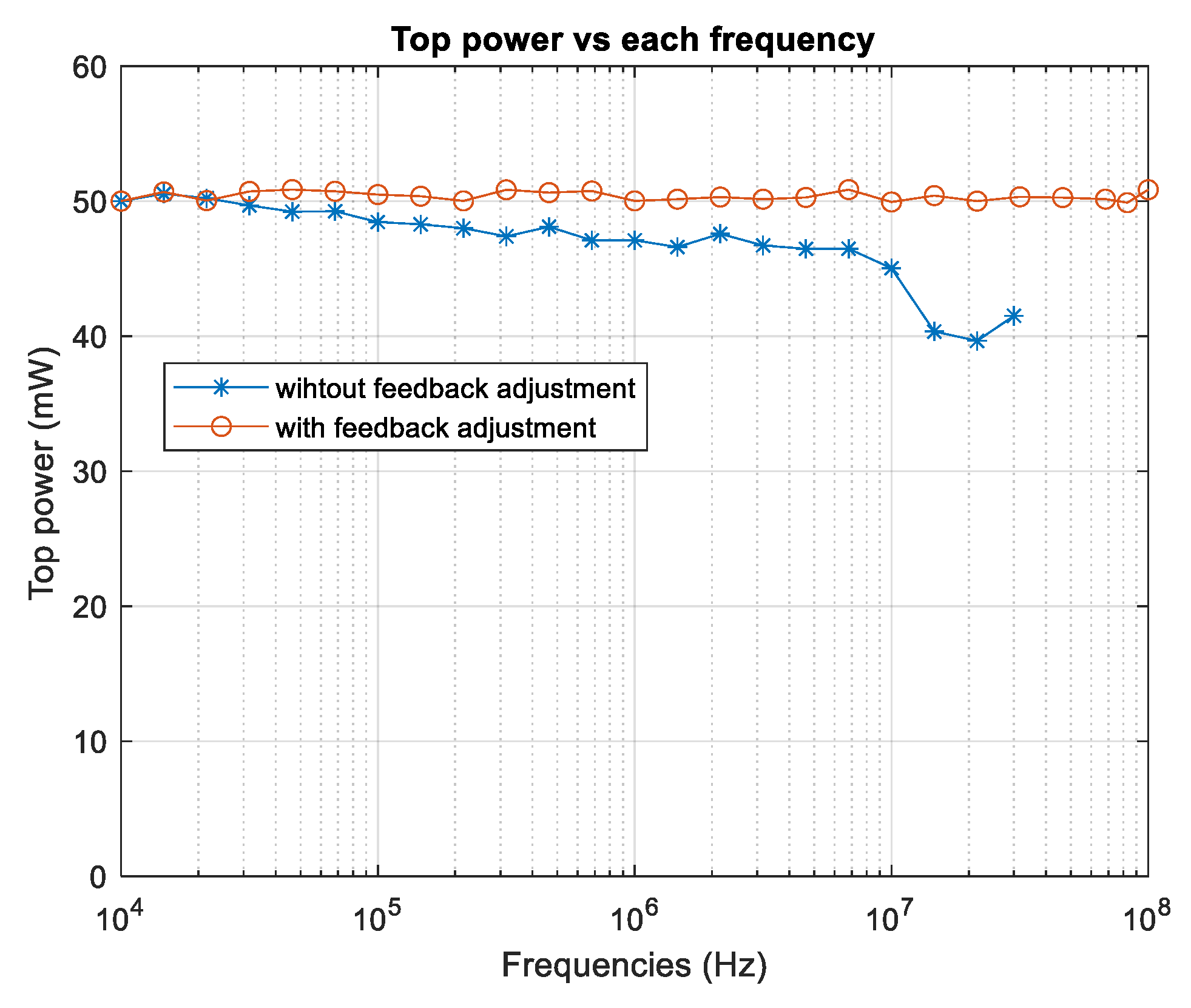
Figure 11.
Duty cycle vs frequency applying the adjustment (circled line) and without applying the adjustment (asterisked line). (Potref = 50 mW, duty cycle = 20%).
Figure 11.
Duty cycle vs frequency applying the adjustment (circled line) and without applying the adjustment (asterisked line). (Potref = 50 mW, duty cycle = 20%).
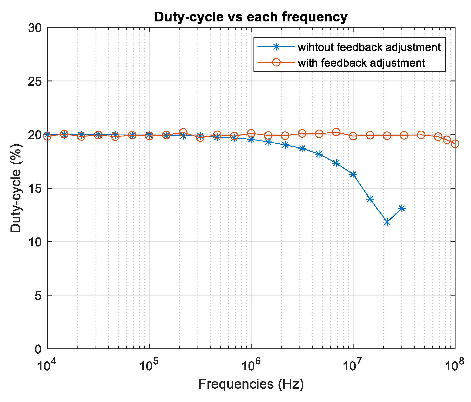
Figure 12.
Top optical power vs frequency applying the adjustment (circled line) and without applying the adjustment (asterisked line). (Potref = 40 mW, duty cycle = 30%).
Figure 12.
Top optical power vs frequency applying the adjustment (circled line) and without applying the adjustment (asterisked line). (Potref = 40 mW, duty cycle = 30%).
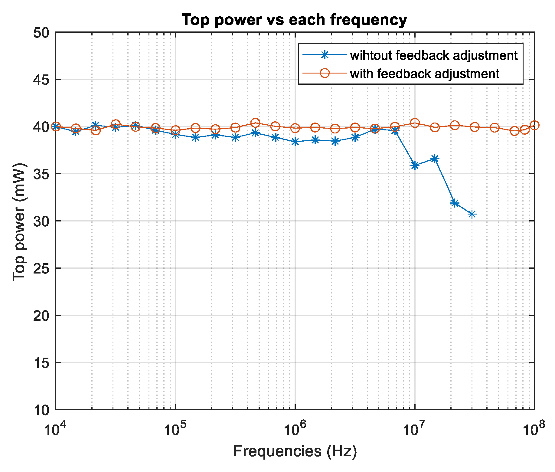
Figure 13.
Top optical power vs frequency applying the adjustment (circled line) and without applying the adjustment (asterisked line). (Potref = 40 mW, duty cycle=30%).
Figure 13.
Top optical power vs frequency applying the adjustment (circled line) and without applying the adjustment (asterisked line). (Potref = 40 mW, duty cycle=30%).
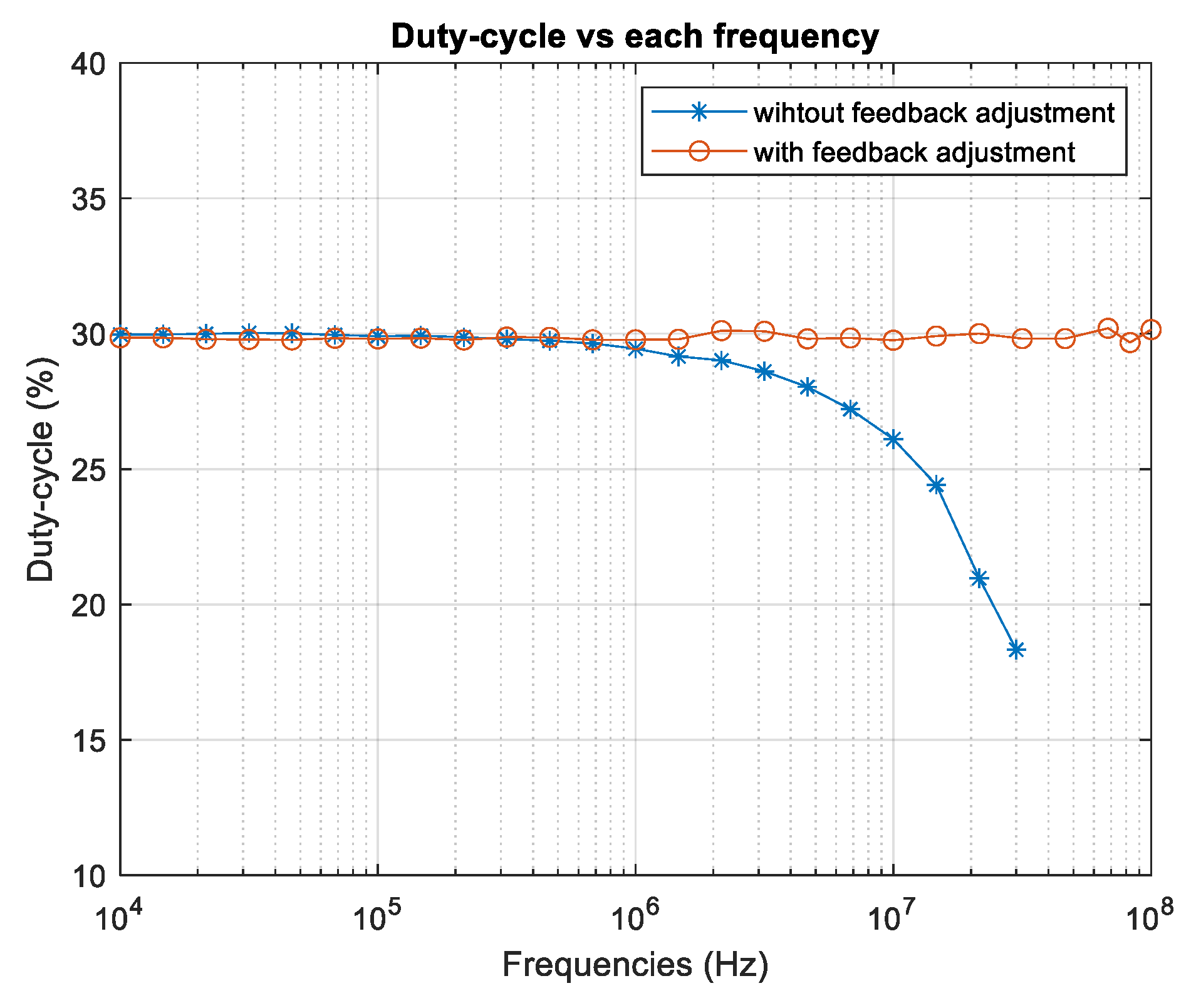

Table 1.
Calculated duty cycle values from equation 1, for a fixed offset of 0.75 V.
| (V) | Duty cycle (%) |
|---|---|
| 1.5 | 19.59 |
| 1.55 | 23.83 |
| 1.65 | 26.94 |
| 1.9 | 31.4 |
Table 2.
NRMSE error calculated from measured optical power values for frequencies ranging from 10 MHz to 30 MHz.
Table 2.
NRMSE error calculated from measured optical power values for frequencies ranging from 10 MHz to 30 MHz.
| References |
(no adjustment) |
(adjustment) |
Relative improve |
|---|---|---|---|
| Pot = 50 mW & Duty = 20% | 18.5% | 0.49% | 97.3% |
| Pot = 40 mW & Duty = 30% | 16.79% | 0.519% | 96.9% |
Table 3.
NRMSE error calculated from measurement duty cycle values for frequencies ranging from 1 MHz to 30 MHz.
Table 3.
NRMSE error calculated from measurement duty cycle values for frequencies ranging from 1 MHz to 30 MHz.
| References |
(no adjustment) |
(adjustment) |
Relative improve |
|---|---|---|---|
| Pot = 50 mW & Duty = 20% | 21.1% | 0.6% | 97.15% |
| Pot = 40 mW & Duty = 30% | 18.56% | 0.52% | 97.2% |
Disclaimer/Publisher’s Note: The statements, opinions and data contained in all publications are solely those of the individual author(s) and contributor(s) and not of MDPI and/or the editor(s). MDPI and/or the editor(s) disclaim responsibility for any injury to people or property resulting from any ideas, methods, instructions or products referred to in the content. |
© 2025 by the authors. Licensee MDPI, Basel, Switzerland. This article is an open access article distributed under the terms and conditions of the Creative Commons Attribution (CC BY) license (http://creativecommons.org/licenses/by/4.0/).
Copyright: This open access article is published under a Creative Commons CC BY 4.0 license, which permit the free download, distribution, and reuse, provided that the author and preprint are cited in any reuse.


