
Submitted:
23 July 2025
Posted:
24 July 2025
You are already at the latest version
Abstract
Regulating the crystallization dynamics of perovskite films is key to improving the effi-ciency and operational stability of perovskite solar cells (PSCs). However, precise regula-tion of the crystallization process remains challenging. Here, we introduce a reactive an-ti-solvent strategy based on the Kornblum reaction to modulate crystallization via in-situ chemical transformation. Specifically, trans-cinnamoyl chloride (TCC) is employed as a single-component anti-solvent additive that reacts with dimethyl sulfoxide (DMSO) in the perovskite precursor solution. The resulting acylation reaction generates carbon-yl-containing products and sulfur ions. The carbonyl oxygen coordinates with Pb²⁺ ions to form Pb–O bonds, which retards rapid crystallization, suppress heterogeneous nucleation, and facilitate the growth of larger perovskite grains with improved film uniformity. Addi-tionally, the exothermic nature of the reaction accelerates local supersaturation and nu-cleation. This synergistic crystallization control significantly enhances the film morphol-ogy and device performance, yielding a champion power conversion efficiency (PCE) of 23.02% and a markedly improved fill factor (FF). This work provides a new pathway for anti-solvent engineering through in-situ chemical regulation, enabling efficient and scala-ble fabrication of high-performance PSCs.
Keywords:
perovskite solar cells
; trans-cinnamoyl chloride
; anti-solvent additive
1. Introduction
Organic-inorganic hybrid perovskite, as an extremely high-performance material, shows remarkable and enormous potential. Perovskite materials have a high absorption coefficient [1] and a long carrier diffusion length,[2] which together enable outstanding power conversion efficiencies (PCEs).[3] Among the various fabrication approaches, solution-processed methods dominate due to their low cost, scalability, and compatibility with large-area production.[4] Nevertheless, achieving uniform, compact, and defect-minimized perovskite films remains a major challenge. A critical factor in this process is the regulation of perovskite crystallization, which is highly sensitive to solvent–antisolvent interactions and additive engineering.
In solution-based fabrication, the careful selection and timing of anti-solvent application are essential to ensure controlled nucleation and high film quality.[5] Over the past decade, researchers have made significant strides in improving film morphology by tuning the composition of perovskite precursors, solvents, anti-solvents, and additives.[6,7] Among these strategies, the use of additives in either the precursor or anti-solvent phase has proven particularly effective in modulating crystallization kinetics and passivating defects.
For instance, Cong et al. introduced 4-morpholine formamidine hydrochloride (MFC) into the anti-solvent phase, where strong hydrogen bonding promoted crystal growth and reduced deep-level defects, resulting in larger grains and improved carrier transport.[8] Similarly, the multifunctional additive o-TB-GDY, featuring high π-conjugation, was shown to enhance crystallization and surface passivation by serving as nucleation seeds and interacting with undercoordinated Pb(0) sites.[9] Wu et al. utilized 1-(2-methoxyphenyl)piperazine hydrochloride (2MPCl) to passivate Pb2+ and halide vacancies via ionic and hydrogen bonding, while also tuning the energy-level alignment between perovskite and PCBM for improved charge extraction and stability [10] Additionally, Li et al. proposed an in-situ functional group conversion strategy using Bis-PEG4-NHS ester, which hydrolyzed during annealing to generate carboxylic acids that enhanced interactions with PbI2 and FAI, thereby reinforcing structural integrity and defect passivation.[11] These efforts underscore the importance of anti-solvent engineering in guiding the crystallization process and improving film quality. However, a more controllable and reaction-driven approach remains desirable.
In this work, we report a novel anti-solvent additive strategy based on the Kornblum reaction, wherein trans-cinnamoyl chloride (TCC) reacts with DMSO in the precursor solution during the annealing step. This acylation reaction produces carbonyl compounds and sulfur ions, which coordinate with Pb2+ and modulate the nucleation kinetics. The exothermic nature of the reaction further accelerates local supersaturation, promoting homogeneous and rapid nucleation. The combined effects lead to the formation of dense, large-grained perovskite films with improved morphology and reduced defects. Devices fabricated using this strategy exhibit significant improvements in both short-circuit current and fill factor, achieving a PCE of 23.02%. Our findings demonstrate a powerful and scalable approach for in-situ chemical regulation of perovskite crystallization, advancing the performance and manufacturability of PSCs.
2. Results
2.1. The Selection of Chemical Reactions
In this work, TCC was chosen to react with DMSO. Studies have shown that the acyl chloride group can react with DMSO, as shown in Figure 1(a). Previous research has indicated that the rate of this reaction is extremely fast.[12] After adding TCC to DMSO, a large amount of heat is rapidly released, and a solid substance is formed within a few minutes. It is envisioned that when TCC is added to chlorobenzene as an anti-solvent and then annealed at 105 oC for 30 minutes, TCC will react rapidly upon contact with DMSO in the perovskite solution, releasing a large amount of heat. This accelerates the rapid nucleation of perovskite, preventing excessive contact with oxygen and water during the annealing process.[13] Meanwhile, the carbonyl group slows down the nucleation rate of perovskite, which is beneficial for improving the quality of the perovskite film.[14] The operation process is shown in Figure 1(b).
2.2. The Influence of TCC on the Morphology of Perovskite
To investigate the influence of TCC as an antisolvent additive on the crystallization behavior of perovskite films, XRD was used to characterize the films treated with different concentrations (0, 10, 20, 30 μL/mL) of TCC. As shown in Figure 2(a), all samples exhibited typical perovskite diffraction peaks near 14.1° (110 crystal plane) and 28.4° (220 crystal plane), and there was no shift in the peak positions, this indicates that the introduction of TCC did not change the crystal structure of the perovskite or induce a phase transition. When the TCC concentration was 10 μL/mL, the intensity of the diffraction peaks increased. However, as the TCC concentration increased, the intensity of the diffraction peaks of the perovskite films showed a significant downward trend, as shown in Figure 2(b). Specifically, the diffraction peak intensities of the unmodified control-group film (0 μL/mL) at the (110) and (220) crystal planes were 6359 and 3288, respectively. When the TCC concentration was increased to 10, 20, and 30 μL/mL, the diffraction peak intensities at the (110) crystal plane were 6866, 6310, and 5898, respectively, and the intensities at the (220) crystal plane decreased to 3979, 3066, and 3040. This result indicates that the introduction of TCC can effectively regulate the crystallization process of perovskite.[15] Combining with solvent chemical analysis, it is speculated that TCC may react with DMSO in the perovskite precursor solution, thereby affecting the formation and growth of crystal nuclei and influencing the crystallization quality of the film.
To further investigate the effect of TCC on the morphology of perovskite films, SEM was employed to characterize the surface morphology of films modified with different TCC concentrations (0, 10, 20, 30 μL/mL) (Figure 3). At a magnification of 50,000, the SEM images clearly revealed the grain distribution of the films, and grain size was quantitatively analyzed using grain statistical software. For the control group (0 μL/mL), the maximum grain size was 1.39 μm, the minimum grain size was 0.26 μm, and the average grain size was 0.68 μm. After 10 μL/mL TCC treatment, the maximum grain size is 1.44 μm, while the minimum grain size slightly increased to 0.29 μm, and the average grain size increased to 0.71 μm. As the TCC concentration further increased, the perovskite grain size began to decrease. With 20 μL/mL TCC treatment, the maximum grain size reduced to 1.34 μm, the minimum grain size decreased to 0.24 μm, and the average grain size declined to 0.65 μm. At 30 μL/mL TCC concentration, the maximum grain size further decreased to 1.29 μm, the minimum grain size dropped to 0.22 μm, and the average grain size reduced to 0.62 μm. This trend was consistent with the XRD results. Combined with XRD analysis, it is hypothesized that at lower concentrations, TCC may interact with DMSO in the perovskite precursor, accelerating nucleation and delaying the crystallization process of perovskite, thereby leading to a smoother perovskite surface and ultimately influencing the film’s microstructure and optoelectronic properties. Figure S1 (a) and (b) show cross-sectional images of the perovskite films, indicating that the thickness of the perovskite layer did not change significantly after TCC treatment. AFM and contact angle measurements were conducted to systematically characterize the changes in perovskite films before and after treatment. AFM results (Figure S2) revealed that the untreated control film exhibited a relatively smooth surface with a root mean square (RMS) roughness of 26.62 nm. In contrast, after 10 μL/mL TCC treatment, the RMS roughness decreased to 24.32 nm. This observation is consistent with the SEM results: the introduction of TCC regulated the perovskite crystallization process, resulting in a denser and more uniform grain size, which led to a smoother surface morphology. Such structural modifications may improve the interfacial contact between the perovskite layer and charge transport layers, thereby enhancing charge extraction efficiency in the device.[16]
2.3. Effect of TCC on the Photovoltaic Performance of PSCs
To investigate the effect of TCC treatment on the electrical performance of PSCs, devices with the structure FTO/SnO2/PVK/Spiro-OMeTAD/Ag were fabricated. Different concentrations of TCC solution (10 μL/mL, 20 μL/mL, 30 μL/mL) were incorporated into chlorobenzene as an antisolvent, and all devices were prepared under the same conditions. Figure 4(a) shows the J-V curves of each group of devices measured under standard AM 1.5G illumination (100 mW/cm2) using a solar simulator. Table S1 lists the performance parameters of the control device and those treated with different concentrations (10 μL/mL, 20 μL/mL, 30 μL/mL) of TCC solution. From the table, the control device exhibited a PCE of 22.53%, an open-circuit voltage (VOC) of 1.12 V, an FF of 80.94%, and a short-circuit current density (JSC) of 24.83 mA/cm2. After treatment with 10 μL/mL TCC antisolvent, the device showed an improved FF of 82.38% and JSC of 25.22 mA/cm2, indicating enhanced charge carrier extraction efficiency. However, the VOC decreased to 1.11 V, while the overall PCE increased to 23.04%. When the TCC concentration was further increased to 20 μL/mL, the device exhibited a JSC of 25.12 mA/cm2, an FF of 83.15%, and a further decreased VOC of 1.09 V, resulting in a maximum PCE of 22.75%. Upon further increasing the concentration, both FF and VOC continued to decline, as shown in Table S1. The JSC, VOC, and FF of these devices showed negligible differences (see Supporting Information, Figure S3). The improvement in FF and JSC may stem from optimized film crystallinity, effectively enhancing charge transport. The significant reduction in VOC after high-concentration TCC treatment may be attributed to the introduction of carbonyl (C=O) and hydroxyl (-OH) groups, which form deep-level defects at perovskite grain boundaries or interfaces, increasing non-radiative recombination losses and thereby lowering Voc.[17]
Additionally, Mott-Schottky (M-S) analysis, transient photocurrent (TPC) decay, and transient photovoltage (TPV) decay measurements were conducted on the devices. The results are shown in Figure 4(b). The built-in electric field of the standard device was approximately 0.88 V, while that of the TCC-treated device was around 0.86 V, indicating a negligible change in the VOC.[18]
After fitting the TPC data, the photocurrent decay response time of the standard device was 3.87 ms, while that of the TCC-treated device was 4.11 ms, showing no significant difference. However, fitting the TPV decay curves revealed that the decay time of the standard device was 0.36 ms, whereas that of the treated device was 0.71 ms (Figure 4(c) and (d)). The significantly shorter photovoltage decay time suggests reduced carrier recombination at the interface of the treated device, which is beneficial for improving device efficiency.[19]
To further investigate the passivation effect of TCC on defects in the perovskite layer of PSCs, the dependence of the device’s JSC and VOC on light intensity (I) was tested. In Figure 4(e), the slope of the linear relationship between VOC and Ln(I) for the control PSC was 1.42, while that of the TCC-treated device was 1.39, indicating a slight reduction in non-radiative recombination in the treated device. Meanwhile, the dark current curves in Figure 4(f) further confirmed the reduction in non-radiative recombination.[20]
2.4. Mechanism of Action of TCC on Perovskite Films
For the device treated with the anti-solvent doped with TCC, the color of the perovskite precursor wet film changes to brown more rapidly, which reflects an accelerated nucleation process. This is beneficial for achieving more uniform crystallization of the perovskite film and improving the film quality. To further investigate the influence of TCC on perovskite nucleation, SEM was used to observe the annealing process of the perovskite, as shown in Figure 5. For the control-group device, the average sizes of the perovskite grains after annealing for 5 and 10 mins are approximately 0.62 and 0.68 μm, respectively. In contrast, for the perovskite treated with the anti-solvent doped with TCC, the grain sizes are about 0.64 and 0.70 μm. The influence on the perovskite grain size during the crystallization process is not significant. From Figure 5(a) and (d), it can be observed that there are many small grains in the perovskite treated with the TCC-doped anti-solvent before annealing. It is speculated that TCC reacts rapidly with DMSO to generate reaction products containing carbonyl groups, and a large amount of heat is released during the reaction. The remaining DMF and DMSO are further evaporated, which promotes the precipitation of perovskite grains. During the subsequent growth process, the oxygen atom in the carbonyl group, with a partial negative charge due to its high electronegativity, can form coordinate bonds with metal cations (such as Pb2+) in the perovskite through electrostatic interaction. This interaction can stabilize the chemical environment around the metal cations, slow down the nucleation rate, make the formed crystal nuclei more uniform, and is beneficial for the growth of high-quality perovskite crystals.
Regarding the effect of TCC treatment on the optical properties of perovskite films, UV-Vis tests were conducted on both the TCC-treated films and the control group films, with the results shown in Figure 6(a). Both the treated and untreated perovskite films exhibited excellent light absorption in the wavelength range of 500–800 nm. Compared to the control group, the perovskite film treated with 10 μL/mL of TCC demonstrated a significantly increased absorbance, which will generate more carriers.[21]
To investigate whether the introduction of TCC affects the energy band of the perovskite film, ultraviolet-visible (UV-vis) absorption spectroscopy was performed on the perovskite film. Figure 6(b) shows the Tauc plot derived from the UV-vis results. After TCC incorporation, the bandgap of the film was 1.551 eV, while that of the control film was 1.567 eV.
Meanwhile, steady-state photoluminescence (PL) and time-resolved photoluminescence (TRPL) tests were conducted on the perovskite thin films treated with 10 mL/mL TCC and the control perovskite thin films, respectively. The results are shown in Figure 6 (c),(d). Figure 6(c) shows the PL spectra of the perovskite thin films before and after TCC treatment. It can be seen that the PL peak intensity of the perovskite thin film modified by TCC is significantly higher than that of the control film. This is because the TCC treatment improves the crystallization quality of the perovskite and reduces the defects.[22]
The measured TRPL data were fitted using a double exponential function, and the obtained fitting parameter values are listed in Table S2. After modification with 10 μL/mL of TCC, the average carrier lifetime (τave) of the perovskite film was 193.26 ns, significantly longer than that of the control film (τave = 68.37 ns). The prolonged carrier lifetime is attributed to the influence of TCC treatment on the nucleation process of perovskite, leading to a reduction in film defects and consequently suppressing defect-induced non-radiative recombination.
2.5. The Impact of TCC on the Stability of PSCs
The stability of perovskite films is closely related to their surface morphology and hydrophobicity. A dense and smooth film structure can effectively block the penetration of environmental moisture, thereby delaying the degradation of perovskite materials and improving the long-term stability of PSCs.[23] To investigate the effect of TCC on the surface properties of the films, water contact angle measurements (Figure S4) show that the control film has a contact angle of approximately 51°, while the film treated with 10 μL/mL TCC shows no significant change in contact angle. This indicates that TCC modification does not significantly alter the surface chemistry of the perovskite film, and its influence on film hydrophobicity is negligible. Combined with AFM data, it is inferred that TCC primarily influences the physical morphology of the film by regulating the crystallization process rather than modifying its wettability through surface chemical alterations.
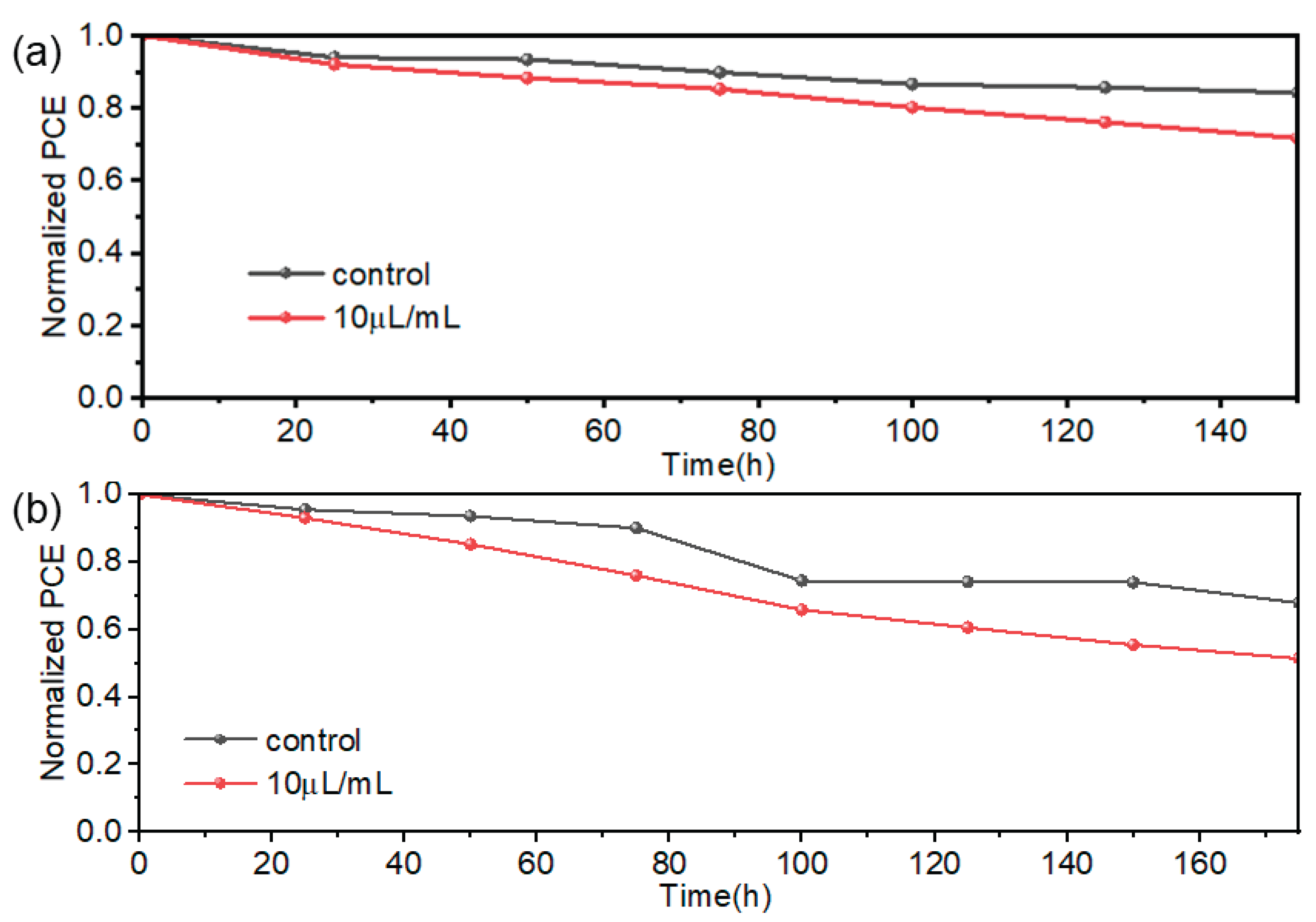
At room temperature, the prepared devices with/without TCC treatment were placed in an air environment with a humidity of approximately 60%±10% and a temperature of 25 °C to test their air stability. The results are shown in Figure 7(a). After being placed for 150 h, the standard device could still maintain 84.2% of its initial efficiency. However, after TCC treatment, the device only retained 71.6% of its initial efficiency. XRD tests also showed that the degree of change in peak intensity and full width at half maximum(FWHM) was relatively larger. After TCC treatment, the stability of the device decreased slightly.
The PSCs were placed in a heating environment (75 °C; N2 atmosphere) in a glove box to study their thermal stability. The results are shown in Figure 7(b). It can be observed that the PSCs treated with TCC have poorer thermal stability than the untreated PSCs. The efficiency of the untreated PSCs remains around 70% of its initial value after 175 h, while that of the PSCs treated with TCC drops to 51% of its initial value after 175 h. The thermal stability of the PSCs after TCC treatment decreases significantly.
The thermal and water stability of the devices both decreased to a certain extent. It is speculated that the reason is that the carbonyl group, as a reaction site, initiates the oxidative degradation of perovskite or accelerates the thermal decomposition of organic components (such as MA+ and FA+).[24] Sulfide ions (S2-), due to their strong nucleophilicity and large ionic radius, easily combine with Pb2+ to form PbS precipitates, which damage the crystal framework of perovskite [25] and ultimately lead to the collapse of the material structure and the decline of performance.
3. Materials and Methods
3.1. Materials
In This Experiment, All Reagents Were Used Directly Without Additional Purificatio. Formamidine acetate (FAAc, 99%), hydroiodic acid solution (57% aqueous solution), methylamine ethanol solution (8% aqueous solution), hydrobromic acid solution (33% aqueous solution), and Trans-cinnamyl chloride(TCC, 95%) were purchased from Aladdin. Lead iodide (PbI2, 99.99%), 2-isopropanol (IPA, 99.8%), acetonitrile (ACN, 99.9%), Lithium bis((trifluoromethyl)sulfonyl), azanide (Li-TFSI, 99.5%) Tributyl phosphate (tBp, 99.99%), lead bromide (PbBr2, 99.99%), cesium iodide (CsI, 99.99%),N, N-dimethylformamide (DMF, 99.9%), dimethyl sulfoxide (DMSO, 99.9%), chlorobenzene (CB) 99.8% purchased from Sima-Aldrich, 2,2’,7,7’ -tetra[N, n-bis (4-methoxyphenyl) amino]-9,9’ -spirodifluorene (99.9%) (Spiro-OMeTAD) purchased from Derthon. All the chemical substances were used in the way they were received, without any further purification.
3.2. Preparation of the PSCs
The fluorine-doped tin oxide (FTO) glass substrate was successively cleaned with ultrapure water, acetone, and ethanol in ultrasonic baths. Each step takes 15 minutes, and then it is placed in a 70°C drying oven to dry for 1 hour. Before spin coating, further clean the FTO substrate with ultraviolet plasma for 10 minutes. To prepare compact SnO2 electron transport layers (ETLs), SnO2 nanoparticles were diluted with deionized water at a ratio of 1:4 to 2.67% to obtain a hydrated tin dioxide solution. Then, at a spin coating speed of 3000 revolutions per minute for 30 seconds with a spin coating acceleration of 2000 revolutions per second 2, a layer of SnO2 was deposited. After spin coating, place the substrate on a heating plate at 150°C for annealing for 30 minutes. For perovskite precursor solutions, 123 mg of methylamine bromide (MABr), 50 microliters of cesium iodide (CsI), 338 mg of methylamine chloride (MACl), 2407 mg of FAI, and 7053 mg of lead iodide (PbI2) were dissolved in 1 ml of a mixed solvent of DMF:DMSO= 9:1, by volume. To prepare perovskite films, 50 microliters of perovskite precursor solution were spin-coated onto the tin dioxide (SnO2) ETL. The coating was first carried out at 1000 revolutions per second for 10 seconds and then at 5000 rpm for 25 seconds. Five seconds before the end of spin coating, slowly add 100 microliters of countersolvent, and then carry out annealing treatment at 105℃ for 30 minutes. The above-mentioned countersolvents refer to the mixed countersolvents of pure chlorobenzene (CB), chlorobenzene, and TCC (with volume ratios of 100:1, 100:2, and 100:3, respectively). Before preparing perovskite films, the electron transport layer was subjected to 15 minutes of ultraviolet ozone treatment to enhance the wettability of the perovskite precursor solution. After cooling to room temperature, 50 microliters of 2,2’,7,7’ -tetra-[N, n-bis (4-methoxy phenyl) amino] -9,9’ - Spiro-OMeTAD solution was spin-coated onto the treated perovskite film at a speed of 4000 revolutions per second for 30 seconds. The preparation method of Spiro-OMeTAD solution is to dissolve 72.3 milligrams of Spiro-OMeTAD in 1 milliliter of CB, and then add 28.8 microliters of tert-butylpyridine (t-BP) and 17.5 microliters of lithium bis (trifluoromethanolimide) (Li-TFSI) to the solution, respectively. 520 milligrams dissolved in 1 milliliter of acetonitrile (ACN). The preparation process of perovskite films and hole transport layers was carried out at room temperature (21 ± 2oC) in a nitrogen atmosphere glove box. Finally, a 120-nanometer silver (Ag) film was deposited as an electrode through vacuum thermal evaporation.
3.3. Characterization and Measurements
X-ray diffraction (XRD) measurements were conducted using Rigaku’s Miniflex600 model instrument. The ultraviolet-visible absorption spectrometer uses the Cary5000 model instrument from Agilent. Under the standard AM 1.5 simulated solar irradiation (SS-F5-3A), using a metal mask with an aperture area of 0.1 cm2, the photocurrent density-voltage (J-V) curve of the device was measured with a Tektronic 2400A source instrument. Ultraviolet-visible (UV-Vis) absorption spectra were recorded on a Cary 5000 spectrophotometer. The water contact angle was measured by a DataPhysics contact angle tester. The top-view and crosssection morphologies of the perovskite films were investigated using field emission scanning electron microscopy (SEM) (Apreo S LoVac, Thermo). The surface roughness by atom force microscopy (AFM) were carried out using Oxford Jupiter XR. Steady-state photoluminescence (PL) (excitation wavelength 460 nm) and time-resolved photoluminescence (TRPL) were conducted with Edinburgh Instruments LTD (FLS 980). Light intensity dependence of the VOC, dark current, transient photovoltage (TPV), and transient photocurrent (TPC) and Mott-Schottky measurements were tested in the dark using an electrochemical workstation (Zennium Zahner, Germany), at room temperature.
4. Conclusions
In summary, this study proposes an anti-solvent reaction strategy, that is, introducing TCC molecules to react with DMSO in the perovskite precursor solution, thereby influencing the nucleation process of perovskite, passivating the internal defects of perovskite, and significantly improving the filling factor and efficiency of PSCs. This work proposes a novel and effective strategy to enhance device efficiency, thereby achieving highly efficient PSCs. In addition, this strategy also has great application potential in other perovskite-based optoelectronic devices.
Supplementary Materials
The following supporting information can be downloaded at the website of this paper posted on Preprints.org.
Author Contributions
Shengcong Wu: Writing – original draft Writing – original draft, Investigation, Formal analysis. Qiu Xiong: Writing – review & editing, Investigation, Formal analysis. Peng Gao: Writing – review & editing, Validation, Resources, Project administration, Funding acquisition, Formal analysis, Conceptualization.
Funding
P.G. acknowledges the financial support from the National Natural Science Foundation of China (Grant nos. 22175180, 52311530673)
Data Availability Statement
Data available on reasonable request from the corresponding author.
Conflicts of Interest
The authors declare that they have no known competing financial interests or personal relationships that could have appeared to influence the work reported in this paper.
References
- Jeong, J.; Kim, B.; Seol, M.J.; et al. Light path management in devices containing halide perovskite materials with a high refractive index. Materials Research Bulletin 2024, 175, 112777. [Google Scholar] [CrossRef]
- Dar, S.A.; Sengar, B.S. Breakthrough in sustainable photovoltaics: Achieving 30.86 % efficiency with innovative lead-free bilayer perovskite solar cells using SCAPS-1D and DFT framework. Solar Energy Materials and Solar Cells 2025, 282, 113352. [Google Scholar] [CrossRef]
- Li, Y. Research progress on preparation methods and photoelectric properties of perovskite solar cell[C/OL]//MOU J, CHEN S. International Conference on Green Communication, Network, and Internet of Things (GCNIoT 2021). Kunming, China: SPIE, 2021, 47. Available online: https://www.spiedigitallibrary.org/conference-proceedings-of-spie/12085/2625439/Research-progress-on-preparation-methods-and-photoelectric-properties-of-perovskite/10.1117/12.2625439.full (accessed on 18 July 2025).
- Chang, J.H.; Liu, K.; Lin, S.Y.; et al. Solution-processed perovskite solar cells. Journal of Central South University 2020, 27, 1104–1133. [Google Scholar] [CrossRef]
- Jung, M.; Ji, S.G.; Kim, G.; et al. Perovskite precursor solution chemistry: From fundamentals to photovoltaic applications. Chemical Society Reviews 2019, 48, 2011–2038. [Google Scholar] [CrossRef] [PubMed]
- Yang, C.; Hu, W.; Liu, J.; et al. Achievements, challenges, and future prospects for industrialization of perovskite solar cells. Light: Science & Applications 2024, 13. Available online: https://www.nature.com/articles/s41377-024-01461-x (accessed on 18 July 2025). [CrossRef] [PubMed]
- Deng, X.; Cao, Z.; Yuan, Y.; et al. Coordination modulated crystallization and defect passivation in high quality perovskite film for efficient solar cells. Coordination Chemistry Reviews 2020, 420, 213408. [Google Scholar] [CrossRef]
- Sun, C.; Jin, L.; Wang, X.; et al. Wide-Bandgap Perovskite and Perovskite/Silicon Tandem Solar Cells through Strong Hydrogen Bonding Interaction. ACS Energy Letters 2025, 10, 2171–2179. [Google Scholar] [CrossRef]
- Shao, C.; He, J.; Ma, J.; et al. Multifunctional Graphdiyne Enables Efficient Perovskite Solar Cells via Anti-Solvent Additive Engineering. Nano-Micro Letters 2025, 17. Available online: https://link.springer.com/10.1007/s40820-024-01630-y (accessed on 12 July 2025). [CrossRef] [PubMed]
- He, R.; Pan, W.; Chen, P.; et al. Synergistic anti-solvent engineering with piperizium salts for highly efficient inverted perovskite solar cells exceeding 25 %. Nano Energy 2024, 131, 110268. [Google Scholar] [CrossRef]
- Liu, M.; Zhang, J.; Qin, S.; et al. Efficient and Stable p–i–n Perovskite Solar Cells Enabled by In Situ Functional Group Conversion. Journal of the American Chemical Society 2024, 146, 32105–32116. [Google Scholar] [CrossRef] [PubMed]
- Fu, D.; Dong, J.; Du, H.; et al. Methanesulfinylation of Benzyl Halides with Dimethyl Sulfoxide. The Journal of Organic Chemistry 2020, 85, 2752–2758. [Google Scholar] [CrossRef] [PubMed]
- Zhang, P.; Gu, N.; Chen, X.; et al. Triethyl phosphate in an antisolvent: A novel approach to fabricate high-efficiency and stable perovskite solar cells under ambient air conditions. Materials Chemistry Frontiers 2021, 5, 7628–7637. [Google Scholar] [CrossRef]
- Li, X.; Zhou, L.; Chen, Q.; et al. Synergistic Carbonyl and Cyano Passivation for Efficient Blade-Coated Perovskite Solar Cells. IEEE Electron Device Letters 2024, 45, 2162–2165. [Google Scholar] [CrossRef]
- Xiang, J.; Cheng, Y.; Zhang, G.; et al. Efficient Carbon-Based Hole-Conductor-Free Printable Mesoscopic Perovskite Solar Cells via a Multifunctional Fluorinated Molecule. Advanced Functional Materials 2024, 34. Available online: https://onlinelibrary.wiley.com/doi/10.1002/adfm.202402816 (accessed on 17 July 2025). [CrossRef]
- Lee, C.M.; Shah, S.H.U.; Ko, K.J.; et al. Impact of Ternary Solvent on the Grain Size and Defects of Perovskite Layer to Realize a Stable Morphology for Efficient Inverted Solar Cells. Solar RRL 2023, 7. Available online: https://onlinelibrary.wiley.com/doi/10.1002/solr.202300604 (accessed on 18 July 2025). [CrossRef]
- Kumar, A.; Gupta, S.K.; Dhamaniya, B.P.; et al. Understanding the origin of defect states, their nature, and effects on metal halide perovskite solar cells. Materials Today Energy 2023, 37, 101400. [Google Scholar] [CrossRef]
- Wu, Y.; Zhang, J.; Luo, J.; et al. Tailoring interface and morphology of TiO2 electron transport layer with potassium bitartrate for high-performance perovskite solar cells. Applied Surface Science 2024, 662, 160139. [Google Scholar] [CrossRef]
- Wang, Y.; Zhou, B.; Han, M.; et al. Formamidine formate as the multifunctional modulator at buried interface for efficient FAPbI3 perovskite solar cells. Nano Energy 2023, 118, 108981. [Google Scholar] [CrossRef]
- Peng, Z.; Wortmann, J.; Hong, J.; et al. Locating Non-Radiative Recombination Losses and Understanding Their Impact on the Stability of Perovskite Solar Cells During Photo-Thermal Accelerated Ageing. Advanced Energy Materials 2025. Available online: https://advanced.onlinelibrary.wiley.com/doi/10.1002/aenm.202502787 (accessed on 18 July 2025).
- Pandey, A.; Vishwakarma, A.; Saini, S.K.; et al. Light-induced micro-strain regulation and charge carrier dynamics of (FA0. 83MA0.17)0.95Cs0.05Pb(I0.83Br0.17)3 hybrid perovskite films. Optical Materials 2023, 146, 114564. [Google Scholar]
- Li, W.; Li, Y.; Wang, D.; et al. Tailored interface molecules for modulating charge carrier dynamics in perovskite solar cells. Nano Energy 2025, 134, 110548. [Google Scholar] [CrossRef]
- Tsai, C.M.; Li, C.F.; Huang, Y.C.; et al. Transparent low moisture permeable coating for perovskite solar cell encapsulation. Surface and Coatings Technology 2024, 482, 130695. [Google Scholar] [CrossRef]
- Sattar, A.; Shahzad, N.; Tariq, M.A.; et al. Carbonyl functional group assisted crystallization of mixed tin–lead narrow bandgap perovskite absorber in ambient conditions. Applied Physics Letters 2022, 121. Available online: https://pubs.aip.org/apl/article/121/7/073901/2834288/Carbonyl-functional-group-assisted-crystallization (accessed on 18 July 2025). [CrossRef]
- Song, J.; Kong, T.; Zhao, Z.; et al. Multifunctional Ammonium Sulfide Enables Highest Efficiency Lead–Tin Perovskite Solar Cells. Advanced Functional Materials 2025, 35. Available online: https://advanced.onlinelibrary.wiley.com/doi/10.1002/adfm.202411746 (accessed on 18 July 2025). [CrossRef]
Figure 1.
(a) Reaction schemes of the Kornblum Reaction. (b) Schematic diagram of performing the Kornblum Reaction during the addition of anti-solvent.
Figure 1.
(a) Reaction schemes of the Kornblum Reaction. (b) Schematic diagram of performing the Kornblum Reaction during the addition of anti-solvent.
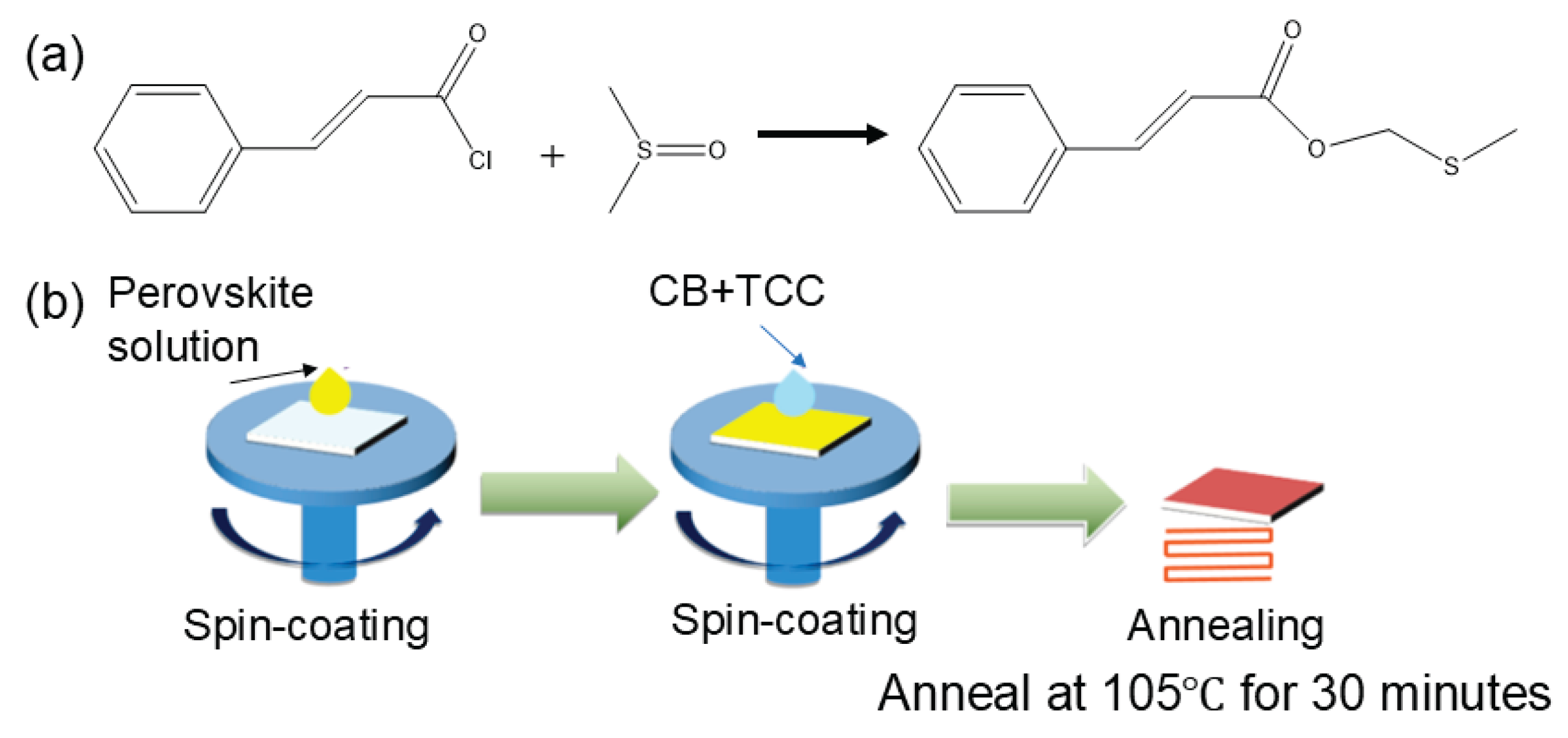
Figure 2.
(a) XRD patterns and (b)(110) peak intensity and half-peak width (FWHM) of perovskite films treated with 0, 10, 20, and 30 μL/mL TCC.
Figure 2.
(a) XRD patterns and (b)(110) peak intensity and half-peak width (FWHM) of perovskite films treated with 0, 10, 20, and 30 μL/mL TCC.
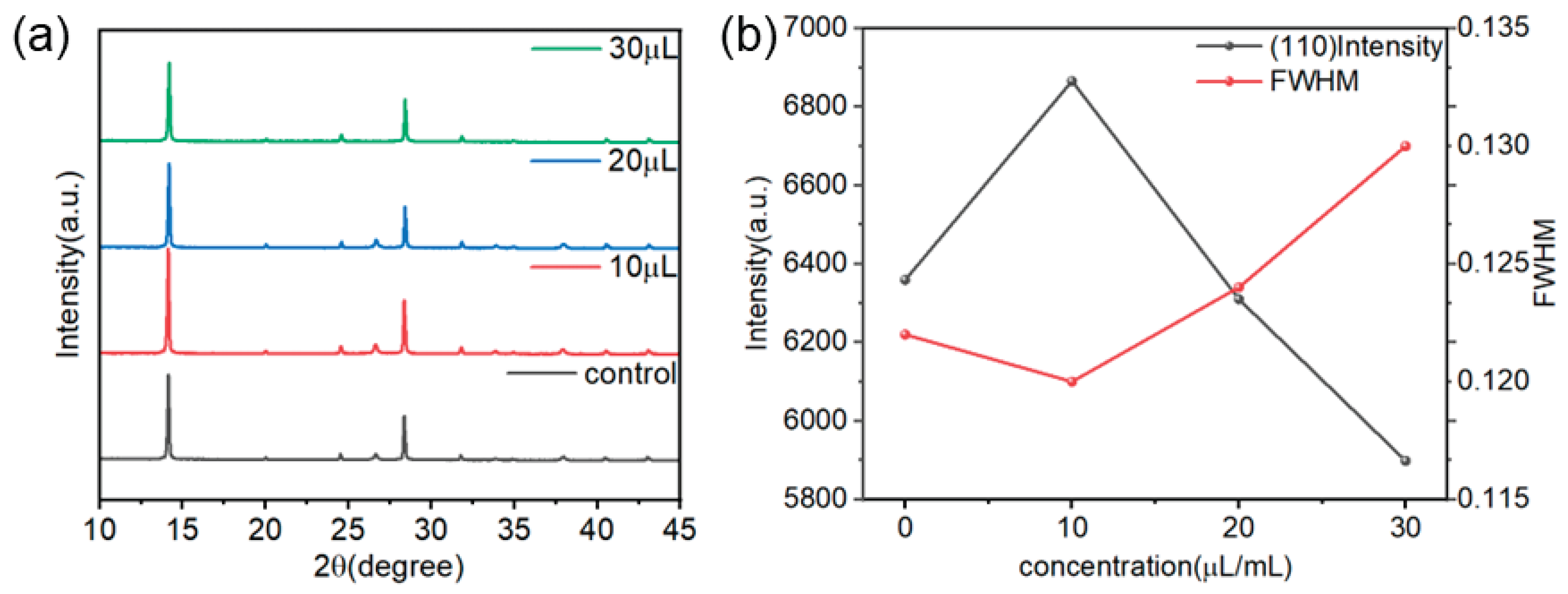
Figure 3.
Topographic SEM images of perovskite films treated with TCC at different concentrations (a) 0 μL/mL, (b) 10μL/mL, (c) 20μL/mL, and (d) 30μL/mL.
Figure 3.
Topographic SEM images of perovskite films treated with TCC at different concentrations (a) 0 μL/mL, (b) 10μL/mL, (c) 20μL/mL, and (d) 30μL/mL.
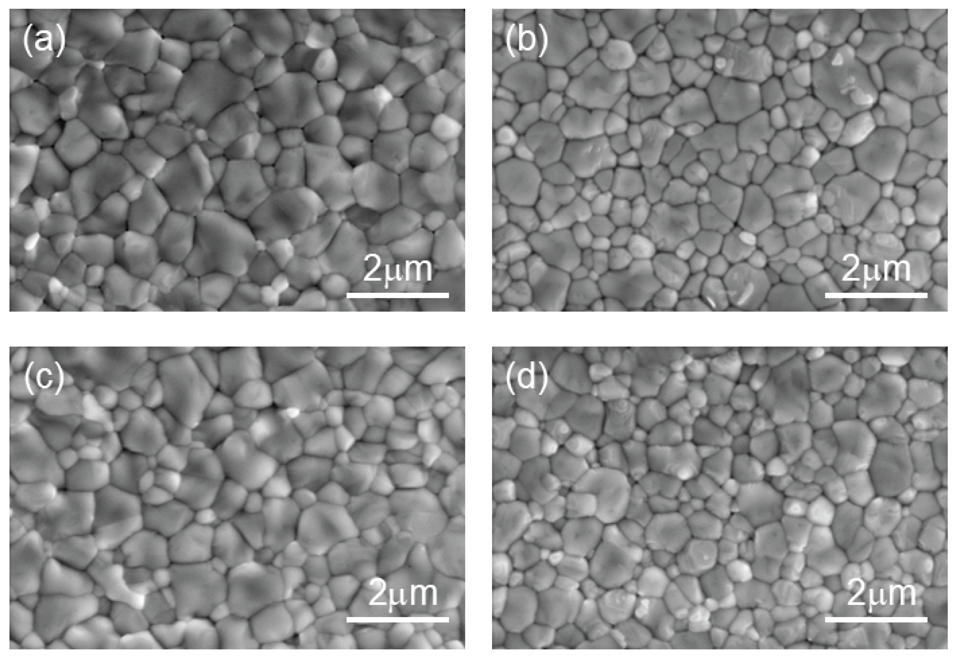
Figure 4.
The effect of TCC treatment on photovoltaic performance. (a) J-V curves of the best-performing devices under each condition. Comparison of (b) M-S plots, (c) TPV, (d) TPC, (e) Light intensity dependence of the VOC, and (f) dark current measurements for perovskite devices before and after BGE-modification.

Figure 5.
(a)-(c) SEM images using TCC as the anti-solvent additive, (a) without annealing, (b) annealed for five minutes and (c) annealed for ten minutes; (d)-(f) SEM images of the control devices (d) without annealing, (e) annealing for five minutes, and (f) annealing for ten minutes.
Figure 5.
(a)-(c) SEM images using TCC as the anti-solvent additive, (a) without annealing, (b) annealed for five minutes and (c) annealed for ten minutes; (d)-(f) SEM images of the control devices (d) without annealing, (e) annealing for five minutes, and (f) annealing for ten minutes.
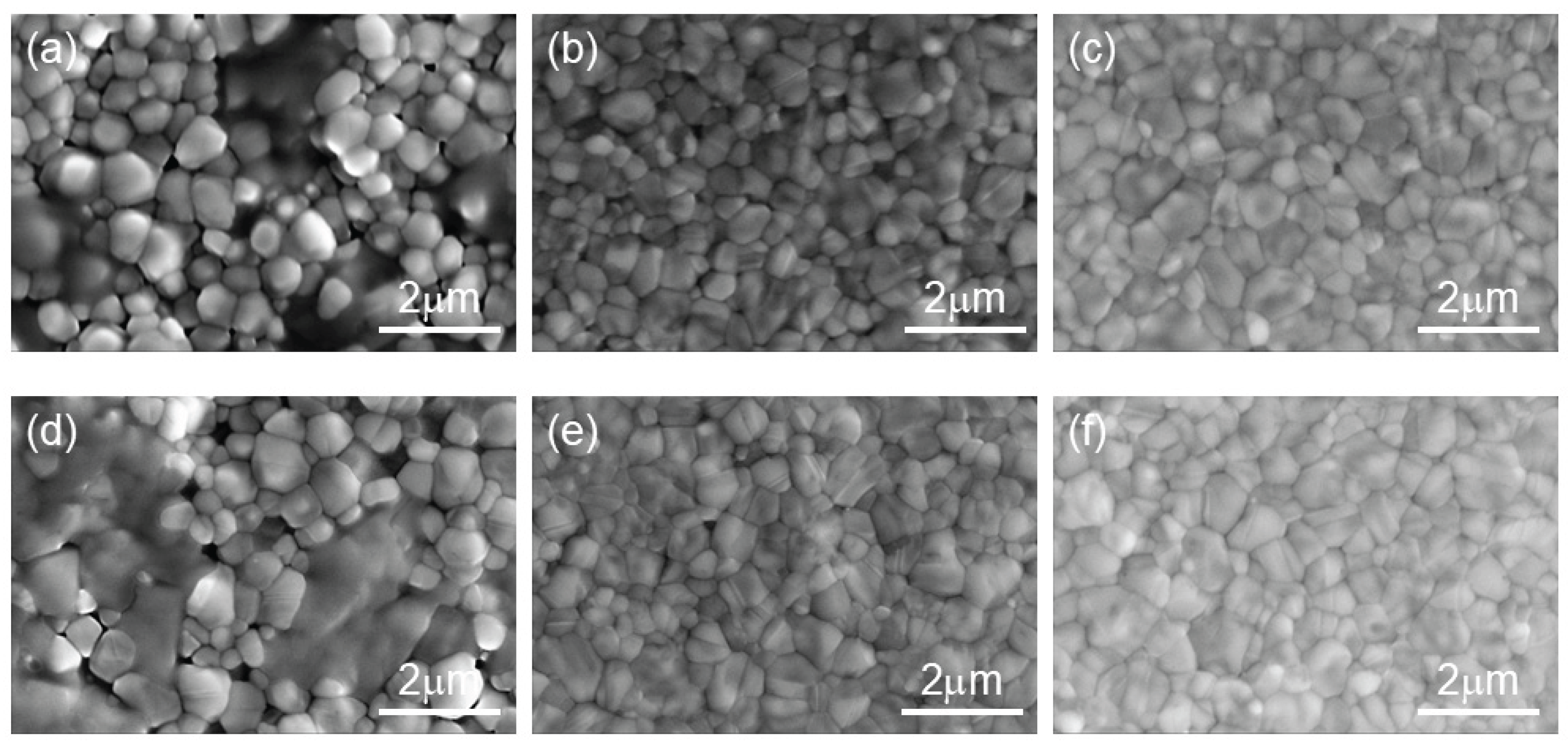
Figure 6.
(a) Absorption spectra, (b) Tauc-plot, (c) PL, and (d) TRPL spectra of perovskite films treated with and without TCC.
Figure 6.
(a) Absorption spectra, (b) Tauc-plot, (c) PL, and (d) TRPL spectra of perovskite films treated with and without TCC.
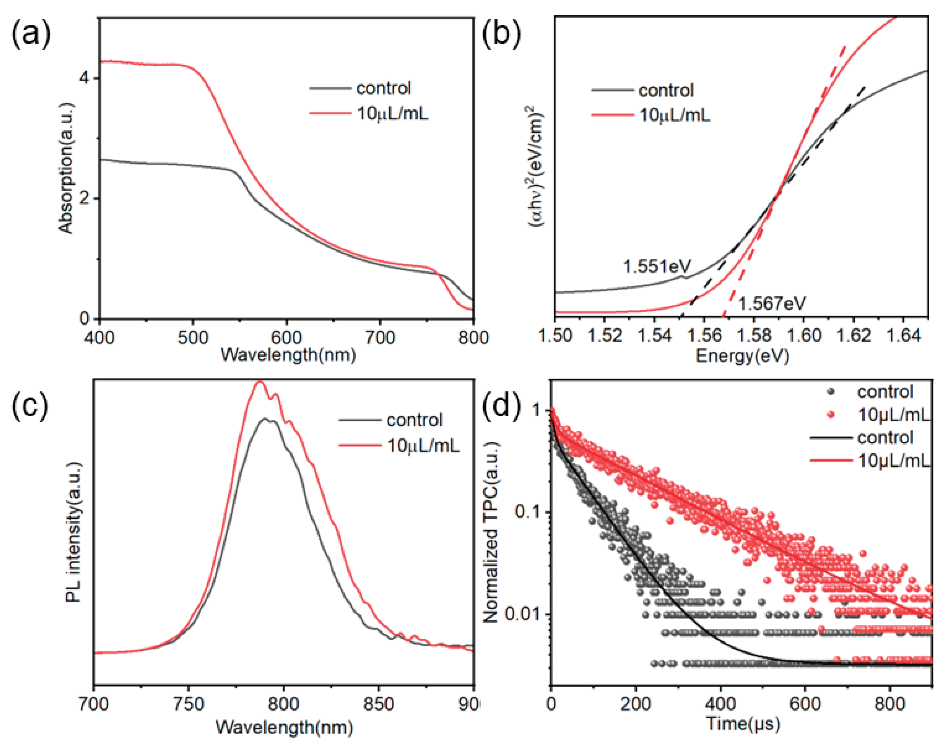
Figure 7.
(a) The air stability and (b) thermal stability of the control and TCC-modified devices.
Disclaimer/Publisher’s Note: The statements, opinions and data contained in all publications are solely those of the individual author(s) and contributor(s) and not of MDPI and/or the editor(s). MDPI and/or the editor(s) disclaim responsibility for any injury to people or property resulting from any ideas, methods, instructions or products referred to in the content. |
© 2025 by the authors. Licensee MDPI, Basel, Switzerland. This article is an open access article distributed under the terms and conditions of the Creative Commons Attribution (CC BY) license (http://creativecommons.org/licenses/by/4.0/).
Copyright: This open access article is published under a Creative Commons CC BY 4.0 license, which permit the free download, distribution, and reuse, provided that the author and preprint are cited in any reuse.


