Submitted:
04 April 2025
Posted:
07 April 2025
You are already at the latest version
Abstract
Novel wide bandgap ZnO, BeO and ZnBeO materials have recently gained considerable interest due to their stellar optoelectronic properties. These semiconductors are being used in developing high-resolution flexible transparent nanoelectronics/photonics and achieving high-power radio frequency modules for sensors/biosensors, photodetectors/solar cells, resistive random-access memory applications. Despite earlier evidence of attaining p-type wz ZnO with N doping, the problem persists to accomplish reproducible p-type conductivity. This issue is linked to charge compensation by intrinsic donors and/ or background impurities. In ZnO : Al (Li), the vibrational features by infrared and Raman spectroscopy have ascribed the presence of isolated AlZn(LiZn) defects; nearest neighbor (NN) [AlZn-NO] pairs; and 2nd NN [AlZn-O-LiZn;VZn-O-LiZn] complexes. However, no firm identification has been established. By integrating accurate perturbation models in a realistic Green’s function method, we have meticulously simulated impurity vibrational modes of AlZn (LiZn) and their bonding to form complexes with dopants as well as intrinsic defects. We strongly feel that these phonon features in doped ZnO will encourage spectroscopists to perform similar measurements to check our theoretical conjectures.
Keywords:
site selectivity of defects in novel ZnO
; Li and Al pair defects
; Raman scattering
; Fourier transform infrared spectroscopy
; Greens function
; lattice dynamics
1. Introduction
High performance electronic devices are essential to the modern world. There is almost no facet of our society that could not be benefitted with the access to better quality and cheaper materials. In the selection process for device applications, scientists and engineers have always preferred those ingredients in a compound which are earth abundant with low toxicity [1,2,3,4,5,6,7,8,9,10,11,12,13,14,15,16,17]. Oxygen (O) is an important member of group VIA elements in the periodic table. It can form wide bandgap (WBG) oxides with different constituents of the group IIB atoms (Be, Mg, Zn, and Cd). Novel composites of are often classified as II-oxides (or II-Os). At ambient conditions most II-Os are highly stable in the wurtzite (wz) or α-phase. They can be transformed to rock-salt (rs) structure under high pressure and to metastable zinc-blende (zb) or β-phase if grown on GaAs and/or Si substrates.
BeO, MgO, ZnO and CdO exhibit many characteristics identical to BN, AlN, GaN, and InN [1,2,3,4,5,6,7,8,9,10,11,12,13,14,15,16,17]. Like BN, the BeO is an exceptionally hard material [18] and revealed unique phonon characteristics different from the other II-Os. As compared to GaN and SiC, the ZnO (with bandgap ~3.3 eV) has a few advantages due to higher ~60 meV exciton-binding energy and availability as a large-size single crystal [17]. Higher cohesive energy, high melting point with strong bonding has implied that the degradation of ZnO based electronic devices might not be an issue for high temperature, T operations. Another niche application accomplished recently is the fabrication of transparent thin-film transistors. Based on transparent conductive oxide (TCO) [19,20,21,22], these transistors are insensitive to visible light where the protective covering to prevent light exposure can be eliminated. The TCO has now emerged as one of the most promising contenders to indium tin oxide (ITO), owing to its vital optoelectronic properties with many benefits, including non-toxicity, availability of abundant raw material, and cost-effectiveness. A few issues in the development of TCO based devices has been the difficulty of achieving reproducible p-type doping. Many reports suggest that the optical properties of ZnO are significantly influenced by the presence of intrinsic defects [23,24,25,26,27,28,29,30,31,32,33,34,35,36] including oxygen-vacancy, zinc-vacancy , zinc interstitials It is academically and technologically important to study the roles of such defects for the development of reliable p-type doping.
In ZnO, group III (B, Al, Ga, and In) dopants have been used as donors to investigate the electronic and vibrational characteristics [23,24]. In II-VI semiconductors, group I (Li, Cu, Ag) and group V (X = N, P, As, Sb) atoms are frequently exploited to make p-type materials. Earlier evidence of N-doped MBE grown ZnO [17,25,26] paved the way of creating p-n-junctions. However, the replication to achieve p-type ZnO has been and still is a challenge. Experimental interpretation of the electronic and vibrational properties for as acceptors, and as donors have varied significantly [25,26]. Except for N, the mass and ionic radii of P, As and Sb are much larger than the O atom [27]. This means that the vibrational modes of isolated will fall in the phonon frequency region of the perfect ZnO. Such vibrational features cannot be observed or analyzed accurately. Interestingly, the ZnO : P samples prepared by different techniques have exhibited the lowest resistivity [17]. Hole concentration and mobilities are usually small due to high activation energies and self-compensation by native impurities. Such intrinsic defects are suggested to create electrically inactive but stable complexes. In simulating the electrical properties of ZnO : X materials, many researchers [37] have considered anti-site defects as they reduce lattice strain caused by mismatch between the ionic radii of X and O. Several reports also indicated that the size difference between X and O initiate deep acceptor states. The difficulty of achieving p-type ZnO : X is caused by charge compensation by intrinsic donors and/or background impurities [37]. In ZnO : Al (Li), besides substitutional Al () (Li ()) defects, the existence of many intrinsic impurities (viz., , , , and anti-site ) are proposed [24,25,26,27,28,29,30,31,32,33,34,35,36]. Force constants describing interaction between an isolated defect and its nearest neighbor (NN) host atoms is considerably higher (lower) than the perfect crystal. Moreover, the involvement of intrinsic impurities is suggested forming different complexes [24,25,26,27,28,29,30,31,32,33,34,35,36] with . The observed vibrational features by Raman scattering and Fourier transform infrared (FTIR) spectroscopy have attributed NN ) and/or 2nd NN defect centers. However, no evidence exists for the involvement of intrinsic impurities in complex centers. Comprehending the role of trivalent B, Al, and monovalent Li dopants in ZnO is crucial. Appraising the association of and with intrinsic defects could play important role in making n-and p-type materials with structural order and required physical properties.
Different epitaxial growth methods are employed in recent years to prepare ultrathin ZnxBe1-xO films [38,39,40,41,42,43,44,45,46,47]. The techniques that have been used included metal organic chemical vapor deposition (MOCVD) [38,39,40], laser ablation [41], CVD, molecular beam epitaxy (MBE), and plasma-assisted PA-MBE [42,43,44,45,46,47], etc. Many characterization efforts are also made for analyzing/monitoring their basic properties [48,49,50,51,52,53,54,55,56,57,58,59,60,61,62,63,64,65,66,67,68,69]. Several measurements have been performed by reflection high-energy electron diffraction (RHEED) [48], Auger electron spectroscopy (AES) [50,51,52], He+ Rutherford backscattering spectrometry (RBS) [53,54,55,56,57,58], atomic force microscopy (AFM) [59,60], high-resolution X-ray diffraction [61,62,63,64] (HR-XRD), transmission electron microscopy (XTEM) [65], photoluminescence (PL) [66,67], absorption, FTIR [60], Raman scattering spectroscopy (RSS) [65,66,67], spectroscopic ellipsometry (SE), [68,69], etc. These experimental methods have not only validated the crystal structures, but also helped evaluating the epifilm thickness, strain, electrical, and optical traits of intrinsic defects. Assimilation of ZnBeO epifilms in MQW and SLs has played important role for the development of various electronic devices including insulated gate bipolar transistors (IGBTs); transparent conductive films for efficient charge carrier transport; ultraviolet (UV) light-emitting diodes (LEDs); high electron mobility transistors (HEMTs); heterostructure field effect transistors; and optoelectronic gas sensors [1,2,3,4,5,6,7,8,9,10,11,12,13,14,15,16,17], etc. Integrating such devices in flexible transparent nanoelectronics/photonics has helped achieving high-resolution medical imaging tools for physicians to diagnose, treat, rehabilitate illnesses, and diseases. Many optoelectronic units are also being incorporated for creating high-power radio frequency modules, sensors/biosensors, photodetectors/solar cells, resistive random-access memory, and surface acoustic wave devices.
To study the lattice dynamics of perfect/imperfect semiconductors, two theoretical approaches are commonly adopted: (i) the microscopic or first-principles methods [70,71,72,73,74,75,76,77,78,79], which start with an ionic potential screened by electron gas for deriving the structural and vibrational properties, and (ii) the macroscopic techniques which employ phenomenological models [80,81,82,83,84,85,86,87] in terms of general interatomic forces. Very few calculations using density functional method (DFT) are known for the lattice dynamics of perfect II-Os [77,78,79]. Absolutely no studies exist on the vibrational properties of isolated and complex defect centers in ZnO. To comprehend the dynamical properties of impurities, many researchers have preferred using macroscopic methods in the framework of Greens function (GF) formalism [80,81,82,83,84,85,86,87]. Careful analysis of local vibrational modes (LVMs) for donors and acceptors in semiconductors has expressed an important revelation. Changes in the NN impurity-host interactions can be ascribed to the electric field created (cf. Section 3) by charged impurities [84,85,86,87]. This important fact is used here for studying the LVMs of acceptor; , donors, and donor-acceptor pairs. The simulation of impurity vibrational modes by GF method requires accurate phonon dispersions of perfect materials. We have adopted a rigid-ion-model (RIM) [88] to calculate the phonon dispersions of zb ZnO, and BeO. Eigen values and eigenvectors of perfect materials are carefully integrated to obtain the GF matrix elements (). Appropriate perturbation matrices () of isolated and complex defect centers are considered to study the impurity vibrational modes. Comparison of theoretical results [81,82,83] with existing Raman scattering and/or FTIR data has helped identifying the nature of different types of defects in zb ZnO.
This paper aims to present systematic results of GF calculations for the dynamical characteristics of various defects in ZnO. Different crystal structures are described in Section 2.1 with the possible existence of intrinsic defects in II-Os. For the lattice dynamics of perfect crystals, a realistic RIM [88] (cf. Section 2.2) is adopted which includes both the short-range and long-range Coulomb interactions. Essential features of RIM are succinctly outlined in Section 2.3, Section 2.3.1, Section 2.3.2 and Section 2.3.3 for evaluating the and matrices [81,82,83]. The GF approach leads to Dyson’s equation to help examining the impurity induced vibrational modes. For ZnO, the calculated results of phonon dispersions and density of states are compared with the experimental data in Section 3.1. In defining , we did not include changes in the Coulomb forces, as their long-range interactions would render the GF approach intractable. Perturbation matrices have included only the changes in atomic masses at impurity sites and the NN force constants. Group theoretic arguments are used to block-diagonalize the and (cf. Section 3) matrices for (i) single isolated defects of symmetry, (ii) NN pair-defects of symmetry, and (iii) complex-defect centers of or symmetry. A modified random element-iso-displacement (MREI) [89,90] model (see Section 3.2) is employed to describe the x-dependent two-phonon mode behavior of ZnxBe1-xO alloys. Impurity modes are evaluated in ZnxBe1-xO at the extreme composition limits (i.e., x → 1 i.e., ZnO:Be and x → 0 for BeO:Zn For closest mass isoelectronic we used the force variation correlation to obtain the impurity modes of acceptor (cf. Section 3.2) and in ZnO. The GF method has predicted LVMs of or donors forming NN pairs with group V (X = N, P,As, Sb) can be used as prospective dopants for creating NNN complexes with , . Our results of LVMs for different impurity centers are valuable and encourage spectroscopists to check our theoretical conjectures. Concluding remarks are presented in Section 4 on microstructures involving group III atoms as donors and group I or V as acceptors.
2. Theoretical Background
2.1. Crystal Structure
At high pressure the ZnO (BeO) material usually occurs in the NaCl-like rs crystal structure with a space group or in a B1 polymorph (see Figure 1 a)). An ultrathin ZnO (BeO) film can exhibit the zb cubic phase if prepared on GaAs and/or Si substrate. The film a mixture of tetrahedral covalent and ionic bonding with space group of or B3 structure [17] (see Figure 1 b)). At ambient conditions of temperature T and pressure P, the epitaxially grown ZnO (BeO) semiconductor material on most substrates occurs typically in a stable wz or B4 structure (see Figure 1 c)) with space group . The NN environment in both the wz and zb materials is very similar.
Intrinsic Defects in ZnO
ZnO is a prototypical n-type semiconductor which exhibits several fascinating physical and chemical properties. While the material is considered valuable for a variety of applications - the realization of many devices has been hindered, however, due to difficulties of achieving reliable and reproducible p-type ZnO. This complexity arises by the strong compensation caused by intrinsic , donors, and/or background impurities. The n-type conductivity of is still being debated. The O-deficient ZnO has always behaved n-type without intentional doping. Theoretical studies [70,71,72,73,74,75,76,77,78,79] have indicated exhibiting the lowest formation enthalpy. Like many deep donors, in ZnO leads to a deep electronic state. At room temperature, cannot be ionized for contributing to n-type conductivity. Thus, the defect energetics of have created huge controversy [17]. We will address some of these issues by simulating the dynamical characteristics of various defect centers involving double dopants (e.g., acceptor atoms from Group I (Li) and donors from Group III (B, Al)) using GF methodology in the framework of a realistic RIM.
2.2. The Rigid-Ion-Model
To treat the lattice dynamics of zb materials in the harmonic approximation, the invariance of potential energy with respect to rigid-body translations, rotations, and symmetry operations require a minimum of two (A, B) NN force constants [91]. For GaAs, this two-parameter force constant model has failed, however, to reproduce the inelastic neutron scattering (INS) results [92] of . This prompted improvement in the oversimplified model by including interactions beyond the NNs. The upgraded RIM proposed by Kunc [88] has accurately explained the INS data of for GaAs [92].
The quantities of interest in RIM are the force constants or dynamical matrices [88]. For zb materials of symmetry the RIM includes short-range interactions () up to 2nd NN with ten parameters (A, B, , , and ; κ = 1, 2). Long-range Coulomb interaction ( is also incorporated using an effective charge parameter . In the harmonic approximation, the lattice vibrations are obtained by solving the following equations of motion [88]:
where represents the dynamical matrix comprising of short- and long range Coulomb interactions. For each mode frequency the components of eigenvectors in Equation (1) satisfy the familiar orthogonality [88]
and closure relations
Once the interatomic force constants (IFCs) , and e)] are evaluated for the zb ZnO [66] and BeO (cf. Section 3.1.2), it is straight forward to simulate using Equation (1).
2.3. The Green’s Function Approach
As stated earlier, the impurity vibrational modes calculations by ab initio methods require heavy computation for isoelectronic CdTe:O [75] defects and it is much more cumbersome for non-isoelectronic (charged) impurities. One must note that in CdTe, no efforts are made by DFT for extracting impurity-host interaction for (d+) donors and (a−) acceptors. In the GF methodology, however, by considering appropriate symmetries of different defect-centers, it is possible to visualize and identify those impurity modes which are optically active and remain localized around the defects. Detailed account of the dynamical properties for perfect/imperfect crystals by GF method has been reported [81,82,83,84] elsewhere. Thus, our discussion to treat the impurity vibrational modes in zb ZnO, will be very brief and only for the purpose of establishing important notations to be used throughout the paper.
2.3.1. The Perfect Lattice Green’s Functions
Using RIM [88], the perfect lattice GF of zb ZnO and/or BeO can be expressed in the matrix notation as:
where the eigenfrequencies of the host crystal are obtained by solving the equation:
The component form of matrix is defined as:
where denotes the number of wave vectors, and is the equilibrium position vector of an atom (). An infinitesimal positive imaginary value to ω is added for producing the retarded GF with a sinusoidal time dependence. The elements of (Equation (5)) can be expressed in terms of its real and imaginary parts [83]. The real part of the matrix is the principal segment of Equation (5), while the imaginary part can be expressed as:
Clearly, Equation (6) becomes zero outside the range of allowed phonon frequencies of the host crystal lattice. For numerical calculations of GFs, we have followed the standard procedures by obtaining first the imaginary part from a sample of wave vectors in the reduced BZ and then determining the real part via the links provided by Kramers - Krönig relations [81,82,83,84].
2.3.2. The Imperfect Lattice Green’s Functions
Like (cf. Section 2.3.1.) of the perfect lattice, one can write the GF matrix elements for the imperfect crystal by using:
or equivalently in the form of a Dyson’s equation
In Equation (8), the term is the perturbation matrix caused by defects. The quantities and represent the mass and force constant change matrices. Since the variation in Coulomb interactions is set to zero = 0, we will consider only the mass change at impurity sites and variation in the NN impurity-host interactions (cf. Section 2.3.3.) in defining for different defect centers. The impurity vibrational modes can be obtained by solving the equation [81,82,83,84]:
Equation (9) may provide the poles of : (i) as a LVM at energy above the maximum phonon frequency of the bulk material, (ii) a gap mode (GM) in the space between acoustic and optic modes and, (iii) an in-band mode falling within the host lattice phonons [60,61,62,63,64,65,66,67]. To simulate the impurity modes of various defect centers we took advantage (cf. Section 2.3.3.) of the symmetry-adapted algorithm [80,81]. This method has helped us comparing theoretical results with the spectroscopic data.
2.3.3. Perturbation Matrices
In any defect calculations, the most important issue has been to give an adequate representation of the impurity perturbation . To study the dynamical behavior of defects (see Figure 2) using GF method, we have appropriately constructed by considering the effects of lattice relaxation to account for the impurity-host interactions. Lattice relaxation in the vicinity of substitutional impurities is estimated using Harrison’s semiempirical bond-orbital model [93]. In terms of Hartee-Fock atomic term values, this method provides simple analytical expressions for the change in impurity-host and host-host bond energies and suggests a computationally efficient and reasonably accurate way of estimating the bond-length distortions. In the framework of RIM, the perturbation matrices are constructed following the method described in Ref. [85,86,87]. To obtain we have used the scaling properties of lattice relaxation caused by different isolated defects along with the trends of short-range interactions in different II-VI and III-V host crystals.
(a) Isolated Defects:
Symmetry
In ZnO the simplest defect responsible for impurity vibrational modes is an isolated substitutional impurity of symmetry (see Figure 2 (a)): where the host lattice atom Zn (κ = 1) or O (κ = 2) [85,86,87] is replaced by an iso-electronic ; acceptor and donor or acceptor, respectively. In the framework of RIM, the perturbation matrix includes both the changes in atomic masses at impurity sites and NN force constants (cf. Section 3). These changes are expressed by the following parameters:
or
for the impurity of mass or occupying either the site κ = 1 or 2, respectively. Following Vandevyver and Plumelle [86] we have considered the impurity-host interaction by a single dimensionless parameter or . The stipulation of = in Eqs. (10b) and (10d) for delineating the matrix hardly affects the high-frequency LVMs. However, imposing this condition on satisfies the rotational invariance requirement, which is explicitly invariant with respect to the translations and crystal-symmetry operations [85,86,87].
The constructions of 15 × 15 full-size and matrices are reported in Ref. [86] for an isolated defect in the zb semiconductors. Considering the symmetry, we have decomposed and into blocks corresponding to the irreducible representations of the group [86]:
For isolated defects, the frequencies of local, gap and in-band modes can be obtained in different irreducible representations by solving the real part of the determinant [86]:
Here, the (ω) of perfect lattice GF is projected on to the defect space, and is the perturbation matrix in each (, E, , and ) irreducible representation. One must note that the impurity modes in , E, and representations are Raman active, while the triply degenerate mode is IR, and Raman active [85,86,87].
(b) NN Pair-Defects:
Symmetry
The perturbation matrix for a NN pair-defect in zb ZnO involves two impurity atoms occupying the sites 1 and 2 (cf. Figure 2 (b)), respectively, causing changes in masses at impurity sites, i.e., = (−) /, = (−) / and force constants between impurity-host atoms, i.e., (1–2, 1–3, 1–4, 1–5), and (2–1, 2–6, 2–7, 2–8). An effective force constant between impurities (≡ 1 − ab + = u + t − ut + ) is included (see Ref. [85,86,87] using ) to account for the changes in u, t of isolated impurities involved in the formation of a pair-defect. The term < 0 (or > 0) signifies stiffening (or softening) between the pair-bond. The pair defect of point group symmetry involves eight atoms which cause the size of impurity space to increase to 24 × 24. The total representation of in the 24-dimensional space group reported by Ludwig [94] is used to block-diagonalize and (ω) matrices with each block along the diagonal belonging to the following irreducible representations:
From group-theoretic analysis, it is perceived that in the representation the impurity atoms in the pair-defect remain stationary. Thus, only and E type modes are optically active. As the degeneracies of mode are lifted at each defect sites, one expects observing four LVM for a pair-defect with very light impurity atoms: two nondegenerate modes due to the movement of impurity atoms along the bond [i.e., ( ← →) and ( → →)] and two doubly degenerate modes as a result of their vibration perpendicular to it [i.e., (↑↓) and (↑↑)], generally with > > > (cf. Section 3.4.). On the other hand, only two (, E) impurity modes will appear for a pair-defect involving a vacancy (or heavy) and a light impurity atom. We will use this perturbation model to account for the experimental results on impurity modes of NN pair-defects (e.g., ; ) and for analyzing atypical Raman scattering spectroscopy data on impurity modes for complex centers involving Al donors and intrinsic defects.
(c) Complex-Defects:
or
Symmetry
The method used for NN pair-defect can be extended to define perturbation matrix for a complex center comprising of three substitutional impurities (see Figure 2(c)) occupying the sites 1 (cation), 2 (anion), and 6 (cation), respectively. Following the case we have considered the mass change parameter at impurity site 6 in terms of = (−) / and the force constant variation between 6–2, 6–9, 6–10, and 6–11 impurity-host bonds by = ( − )/ = ( − )/ = 1 − . Like the NN pair-defect, an effective force constant between the impurity-atoms 2–6 (≡) is also included. The point group symmetry for such a complex defect center is if = , otherwise The complex causes the size of defect space to increase to 33 × 33. By constructing a total representation of / in the 33-dimensional space, we have block-diagonalized and matrices belonging to the following irreducible representations [85,86,87]:
and
with , , and ( and ) types of vibrations being optically active. This perturbation model will be used to account for the experimental results on impurity modes of NNN pair-defects (e.g., ; ) and for analyzing the atypical Raman scattering spectroscopy data on impurity modes of complex centers involving Al donors and intrinsic defects (see Section) in Al-doped ZnO.
3. Numerical Computations Results and Discussion
3.1. Theoretical Framework of Phonons
Significant interest has gained recently in ZnO due to its potential use in developing devices for transport electronics and UV optoelectronics. Lattice dynamics plays an important role for comprehending electron transport and interaction of phonons with charge carriers. In polar semiconductors, when free charges are excited high in the conduction band, they relax to the ground states via Fröhlich interaction involving LO phonons. One, therefore, expects the dynamics of phonon population strongly impacting the performance of high-speed electronic devices. Despite extensive measurements for assessing the structural and electrical properties of doped wz materials, there are limited spectroscopic studies available on the zb ZnO for appraising their phonon, bonding, and impurity vibrational characteristics.
As the cohesive energy of ZnO is very close to that of the zb material, it can be grown either in wz and/or zb phases. The wz ZnO with 4 atoms/unit cell and space group is a non-centrosymmetric having 12 normal modes as compared to 6 modes in the zb () lattice with 2 atoms/unit cell. Based on group theory, the total representation of zone center optical phonons can be classified as [66]:
where the superscript 2 on and indicates double degeneracy. Contrary to zb, the normal modes of wz phase are linked to different symmetry representations. Among the 12 modes, one set of and are acoustic, the other nine phonons are optical. At Γ point, the acoustic modes vanish while one , two , one , and two optical phonons are non-vanishing. The polar , modes are Raman and IR active while the nonpolar phonons are only Raman active. The and modes exhibit in-plane atomic vibrations, whereas the atoms in modes vibrate along the c-axis (see Figure 3).
Lattice Dynamics of ZnO
The phonon dispersions of wz ZnO material are measured using INS and calculated by first principles method [65]. At a few critical points, the phonon modes are also achieved by IR reflectivity/absorption and Raman scattering spectroscopy. In zb ZnO, the phonon dispersions are displayed in Figure 4a) by RIM along high symmetry (Γ→X→ K→ Γ→ L→ X→ W→ L) directions in the BZ. Theoretical results have agreed reasonably well with RSS [95] data. Simulated one-phonon DOS is shown in Figure 4b).
Inspection of Figure 4 ab) confirms that the optical and acoustical phonons of zb ZnO are affected by the light O (16.0 amu) and heavier Zn (65.38 amu) atomic masses, respectively. First and second peaks in the low-frequency region of (see Figure 4 b)) are associated to average values of the and modes while two high-frequency peaks correspond to the average and phonons, respectively. In the phonon gap (~275–405 cm−1) between the maximum acoustic and minimum optical phonons is caused by the large mass difference between the O and Zn atoms. In Table 1, we have listed the main phonon frequency features at high critical points for both the wz and zb ZnO materials.
Comparison of these phonon values have exhibited interesting traits. In both structures the range of mode frequencies and gaps between the acoustic and optical phonons are quite similar. These equalities have helped us comparing GF calculation of impurity modes for different defect centers in zb ZnO with the Raman scattering data of wz material. The simulation of impurity modes (LVMs and GMs) reported in Section 3.3 has followed the typical procedures reported elsewhere [85,86,87]. In short for the zb ZnO, BeO materials, the RIM eigenvalues and eigenfunctions at 64, 000 points in the BZ are incorporated for computing the GF matrix elements . The phonon dispersions and DOS of zb ZnO have served as a guide to interpret experimental data of LVMs and GMs for different defect centers in wz material.
3.2. Chemical Trends of Impurity-Host Interactions
The dynamical properties of defects in wz ZnO are studied by Raman scattering spectroscopy for the closest mass ; and donors. Similar measurements also exist for the sodium magnesium and aluminum dopants [24,25,26,27,28,29,30,31,32,33,34,35,36]. A careful analysis of the LVMs for charged defects in zb crystals have conveyed a very important revelation. The estimated changes in the NN force constants are ascribed as the effects of electric field produced by charged impurities [85,86,87]. This effect instigates redistribution of charge around isolated impurity for producing changes in the covalency (or ionicity) between the impurity-host bond. In II-VI materials, a simple empirical relationship providing corrections to in the NN force constants of closest mass isoelectronic Mg (i) and donor Al () or isoelectronic Be (i) and acceptor Li () occupying the cation sites exhibit the following trends [85,86,87]:
Similarly, the values of between the closest mass isoelectronic S (i) and an acceptor P () occupying the anion site reveal:
and we expect
for an isoelectronic S (i) and a donor Cl () occupying the anion sites, respectively. Absolute values of relative variations in and for the single charged (, ) and isolectronic (i) defects producing LVMs in II-VI and III-V compounds are seen within 30 %. Although these correlations are found independent of the long-range Coulomb forces, we have strongly argued that the charged impurities in semiconductors affect only the short-range forces via the redistribution of electron-charge density. These arguments are supported in a self-consistent super-cell study by Baraff et al., [76] where the electronic-charge density contours are simulated for both the perfect GaP and imperfect GaP:O systems to mark the evidence of a weak bonding between the –Ga bonds.
We believe that these unique and valuable trends in force variations (Equations 16 ad)) are significant to serve as a good starting point to make predictions of impurity modes for both the isolated and complex defect centers in zb ZnO. In Section 3.2.1 we will start to verify these arguments in learning the composition dependent long-wave-length optical phonons in alloys. Results of impurity modes reported in Section 3.3 by GF simulations for isolated and complex defect centers in zb ZnO will be compared/contrasted against the existing Raman scattering and FTIR data [24,25,26,27,28,29,30,31,32,33,34,35,36].
Long-Wavelength Optical Phonons in Alloys
To understand the composition dependent long-wave-length optical phonons in ternary alloys, we have used the MREI model [89,90]. This model assumes that x portion of the NN of O has Be atoms with 1-x share of Zn atoms. The NN of Be and Zn has O-atoms. Long-range Coulomb interaction is included as a local field. The necessary parameters (cf. Table 2) of constituting bonds (Be-O; Zn-O; Be-Zn) are obtained using the atomic masses; effective charges by relating them to , phonons and LVM as well as in-band/gap mode frequencies.
The LVM and in-band/gap mode obtained by GF method at the extreme composition limits x → 0 for isolated (in zb ZnO) and x → 1(in BeO) defects are used for evaluating the necessary MREI parameters:
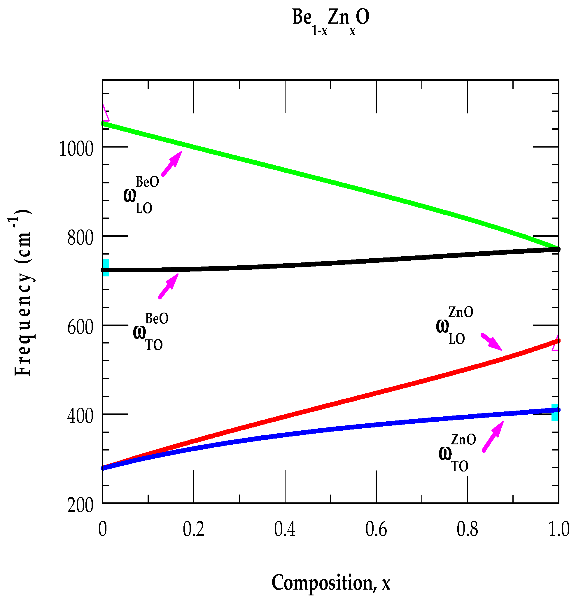
The model [90] offers a simple criterion for predicting the two-phonon mode behavior for alloys. If , , are the masses of A, B, C atoms (< of A and C having < then, alloy displays a two-phonon-mode behavior. For A = O; B = Be and C = Zn, the above criteria is valid for . Calculations of x-dependent optical phonons displayed in Figure 6) with parameter values listed in Table 2 (a,b) have confirmed the two-phonon mode behavior. Our results are in very good agreement with a recent study reported for the wz alloys [96].
Figure 5.
Simulated two-phonon mode behavior of alloys based on modified random-iso-displacement model.
Figure 5.
Simulated two-phonon mode behavior of alloys based on modified random-iso-displacement model.
3.3. Vibrational Modes of Isolated Defects in zb ZnO
For the GF methodology (cf. Section 3.2) is used to calculate the impurity vibrational modes of isoelectronic and defects in the extreme composition limits: x → 0 (ZnO:Be) and, x → 1 (BeO:Zn). By carefully including appropriate perturbations for lighter in zb ZnO has predicted a high frequency LVM at ~ 780 cm-1 and in-band impurity mode at lower frequency ~ 280 cm-1 for heavier in zb BeO.
Impurity Modes of Closest Mass Isoelectronic, Donor and Acceptor on Zn-Site in ZnO
Calculation of LVM for has helped us estimating the impurity vibrational modes of closest mass lithium acceptor () and boron donor in zb ZnO. Besides considering the mass change at impurity sites, the GF simulations are performed by including appropriate force variations using Equations 16 ab). In Table 3, we have listed the predicted values of LVMs and GMs for several isolated impurity atoms occupying Zn (O) site in the zb ZnO. The impurity vibrational modes are estimated from the results of real and imaginary parts of det |I- displayed as a function of frequency. We have used Equation 12) and Figure 6 ac) for assessing LVMs and GMs when the real part of det |I- crosses to zero.
Figure 6.
Calculated real (black line) and imaginary (green line) parts of the det | I − GoP | (cf. Section 2.3.3) in the representation. Crossing zero of the real det |I − GoP| provides local and gap modes (see: Table 3) for (a) and (c) ZnO.
Figure 6.
Calculated real (black line) and imaginary (green line) parts of the det | I − GoP | (cf. Section 2.3.3) in the representation. Crossing zero of the real det |I − GoP| provides local and gap modes (see: Table 3) for (a) and (c) ZnO.
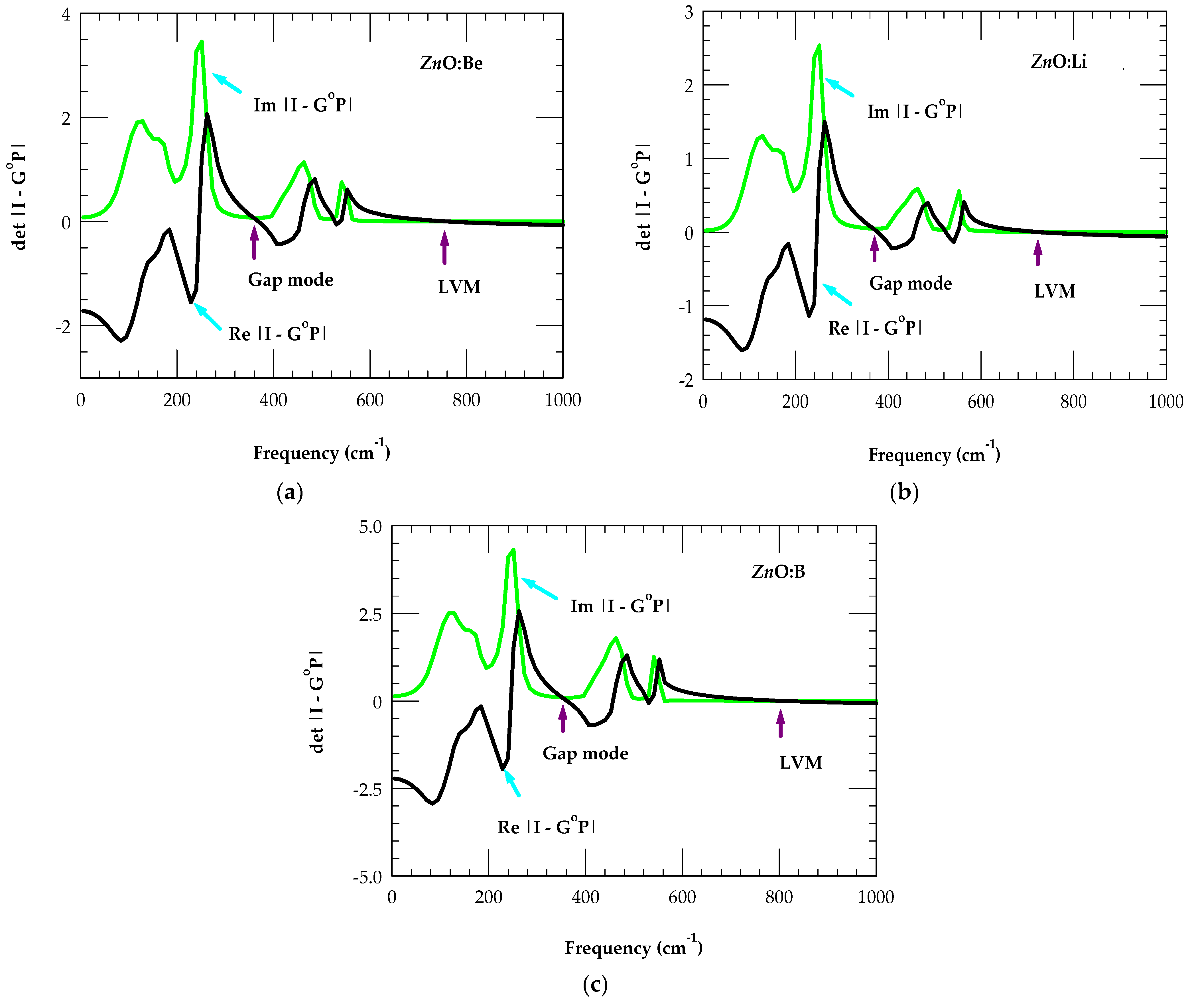
The results reported in Table 3, and Figure 6 ac) have revealed interesting characteristics. Although the mass of Li (B) is lower (higher) than that of the isoelectronic Be, the GF calculations predicted LVM at lower (higher) ~740 cm-1 (~804 cm-1) frequency for (. The shifts in impurity modes are linked to NN force constant variations causing softening (stiffening) between the ( bonds. While no measurements of impurity modes exist for these defects in the zb ZnO, our results have agreed very well with the Raman scattering (FTIR) studies of Li- (B) doped [27,28] wz ZnO nanocrystals for Li-O (B-O) mode in the LiO2 (BO2) configuration. Besides LVMs, each light impurity in zb ZnO predicts the GM with its frequency decreasing with the increase of mass from → → . These results have provided strong corroborations to an earlier study by Vandevyver and Plumelle [86] where the authors have predicted both the LVMs and GMs for light impurities occupying the Zn-sites in zb ZnS.
Similar calculations of impurity modes are displayed in Figure 7 ac) for the closest mass Mg isoelectronic , Na acceptor () and Al donor in zb ZnO.
With respect to the changes in for () and have indicated softening (stiffening) between the -O (-O) bonds. Thus, only donor has exhibited the LVM while all impurities (, ) indicated the possibilities of GMs. Consistent with closest mass Li, Be and B dopants the frequencies of GMs are shown decreasing with the increase of impurity mass . In the absence of experimental results for zb ZnO, our theoretical simulations of defect activated optical phonons (see Table 3) are compared reasonably well with the limited Raman scattering and/or FTIR data in wz ZnO. In some reports [24,25,26,27,28,29,30,31,32,33,34,35,36] many researchers have quoted the impurity activated optical phonons for and other impurities (Mn, Co and Fe) as LVMs. Such assignments are inaccurate and need to be corrected.
3.4. Impurity Vibrational Modes of in ZnO
Like II-VI semiconductors, the double doping with group III (Y = B, Al, Ga and In) () atoms and group V (X = N, P, As and Sb) impurities in ZnO, can create NN “donor-acceptor” - pairs of symmetry. A simultaneous doping of Li with group III defects can also form 2nd NN -O- complex centers of symmetry. In Table 4, we have reported results of our GF calculations for the LVMs of different impurity complex centers. In zb ZnO, the calculations of NN () and 2nd NN () pairs are performed by keeping the same values of force constants as estimated for isolated defects. Interesting trends perceived in the simulations of LVMs are worth recognizing: (a) The NN - pairs of symmetry reveal causing only 2 LVMs linked to the vibration of - the other 2 modes associated with fall, however, into the optical phonon regions. The average frequency of LVM stays nearly constant when heavier impurities are involved in the pair. (b) The 2nd NN - pairs of symmetry confirmed causing six vibrational modes three each of the light ( donor and isotopic acceptors, respectively. The average frequency of the splitting of LVM for each isolated defect in the complex center falls well within their triply degenerate values.
These, outcomes have provided valuable evidence for the site selectivity of different light substitutional defects from groups I and III as well as their atomic interactions with the host lattice atoms in zb ZnO. This information will be quite effective for assessing the evidence of microstructural configuration of NN and 2nd NN complexes, particularly the creation of impurity pairs involving double dopants. Like many II-VI semiconductors, the vibrational study by GF method has provided support to the association of different impurities with intrinsic (; ) defects. We feel that the LVMs of different impurity complexes in zb ZnO will encourage spectroscopists to use FTIR and/or Raman scattering spectroscopy to check our theoretical conjectures.
4. Concluding Remarks
Many, scientists and engineers working in nanoelectronics/photonics have paid attention in recent years to discover novel materials for designing devices to satisfy the growing needs of high-T electronics, healthcare, photovoltaic and automotive industries. Devices based on WBG GaN, and ZnO ~3.37 eV) can be used to cover nearly the same wavelengths. However, the ZnO material of exciton binding energy (~ 60 meV) has been preferred in fabricating laser diodes with lower threshold by excitons for operation at high efficiency and temperature. Despite many valuable characteristics of ZnO, there has been an important issue of achieving reproducible p-type conductive layers. Doping of ZnO by monovalent lithium can be a prospective approach to compensate n-type conductivity by intrinsic defects and intentionally doped trivalent (B, Al) atoms [17]. In ZnO: Al (Li), although SEM and PL measurements [65,66,67] are used for determining the morphology and investigating their optical properties, only limited impurity vibrational features exist by FTIR and Raman spectroscopy [24,25,26,27,28,29,30,31,32,33,34,35,36,37,38]. In the frame work of a realistic RIM [88] and by integrating accurate perturbation models in the Green’s function method, we have meticulously simulated impurity vibrational modes of and their bonding of forming NN ] pairs; and 2nd NN complexes. We strongly feel that these phonon characteristics in doped ZnO material will encourage spectroscopists to perform similar measurements to check our theoretical conjectures.
Author Contributions
DT has been responsible for the conceptualization, developing methodology, investigations and for computational analysis of the results reported here. As a supervisor PB provided valuable feedback, checked, reviewed, and edited the original draft.
Funding
This research has received no external funding.
Institutional Review Board Statement
Not applicable. There are no experiments involving human tissue or any ethical issues.
Data Availability Statement
The data that support the findings of this study are available from the author upon reasonable request.
Acknowledgments
The work reported here was done at the Physics Department, University of North Florida (UNF) in Jacksonville, FL 32224. The author DT would like to thank Deanne Snavely, Dean College of Natural Science and Mathematics at Indiana University of Pennsylvania, for the travel support which made this research possible. DT would also like to thank Jason Haraldsen of the UNF, Physics Department for providing the Origin software (2017) for data analysis and graphing.
Conflicts of Interest
The author declares having no financial and/or competing interests.
References
- Udayagiri, H.; Sana, S.S.; Dogiparthi, L.K.; Vadde, R.; Varma, R.S.; Koduru, J.R.; Ghodake, G.S.; Somala, A.R.; Boya, V.K.N.; Kim, S.-C.; Karr, R.R. Phytochemical fabrication of ZnO nanoparticles and their antibacterial and anti-bioflm activity. Scientific Reports 2024, 14, 19714. [Google Scholar] [CrossRef] [PubMed]
- Mutukwa, D.; Taziwa, R.T.; Khotseng, L. A Review of Plant-Mediated ZnO Nanoparticles for Photodegradation and Antibacterial Applications. Nanomaterials 2024, 14, 1182. [Google Scholar] [CrossRef] [PubMed]
- Jha, S.; Rani, R.; Singh, S. Biogenic Zinc Oxide Nanoparticles and Their Biomedical Applications: A Review. Journal of Inorganic and Organometallic Polymers and Materials 2023, 33, 1437–1452. [Google Scholar] [CrossRef] [PubMed]
- Natu, K.; Laad, M.; Ghule, B.; Shalu, A. Transparent and flexible zinc oxide-based thin-film diodes and thin-film transistors: A review. J. Appl. Phys. 2023, 134, 190701. [Google Scholar] [CrossRef]
- Hazarika, R.; Kalita, B. Site selective behavior of B, C and N doping in MgO monolayers towards spintronic and optoelectronic applications. Materials Science in Semiconductor Processing 2023, 162, 107514, Balu, K.; Kaliyamoorthy, S.; Mani D.; Aguiar, A.; Sobral, M.C.M.; Muthuvel, I.; Kumaravel, S.; Avula, B.; Sobral, A.J.F.N.; Ahn, Y.-H., Porphyrins and ZnO hybrid semiconductor materials: A review, Inorganic Chemistry Communications 2023, 154, 110973.. [Google Scholar] [CrossRef]
- Wang, Z.L. Towards Self-Powered Nano systems: From Nanogenerators to Nano piezotronics. Adv. Funct. Mater. 2008, 18, 3553−3567. [Google Scholar] [CrossRef]
- Tian, W.; Lu, H.; Li, L. Nanoscale Ultraviolet Photodetectors Based on One-Dimensional Metal Oxide Nanostructures. Nano Res. 2015, 8, 382−405. [Google Scholar] [CrossRef]
- Willander, M.; Nur, O.; Zhao, Q.X.; Yang, L.L.; Lorenz, M.; Cao, B.Q.; Zuniga-Perez, J.; Czekalla, C.; Zimmermann, G.; Grundmann, M.; et al. Zinc Oxide Nanorod Based Photonic Devices: Recent Progress in Growth, Light Emitting Diodes and Lasers. Nanotechnology 2009, 20, 332001. [Google Scholar] [CrossRef]
- Consonni, V.; Briscoe, J.; Karber, E.; Li, X.; Cossuet, T. ZnO Nanowires for Solar Cells: A Comprehensive Review. Nanotechnology 2019, 30, 362001. [Google Scholar] [CrossRef]
- Zhu, L.; Zeng, W. Room-Temperature Gas Sensing of ZnO Based Gas Sensor: A Review. Sens. Actuators A 2017, 267, 242−261. [Google Scholar] [CrossRef]
- Abdullahi, Y.Z.; Ersan, F. Stability and electronic properties of XO (X = Be, Mg, Zn, Cd) biphenylene and graphenylene networks: A first-principles study. Appl. Phys. Lett. 2023, 123, 252104. [Google Scholar] [CrossRef]
- Pushpalatha, C.; Suresh, J.; Gayathri, V.S.; Sowmya, S.V.; Augustine, D.; Alamoudi, A.; Zidane, B.; Albar, N.H.M.; Patil, S. Zinc Oxide Nanoparticles: A Review on Its Applications in Dentistry, Nanoparticles. Front. Bioeng. Biotechnol. 2022, 10, 917990. [Google Scholar] [CrossRef] [PubMed]
- Sharma, D.K.; Shukla, S.; Sharma, K.K.; Kumar, V. A review on ZnO: Fundamental properties and applications. Materials Today: Proceedings 2022, 49, 3028–3035. [Google Scholar] [CrossRef]
- Zahoor, R.; Jalil, A.; Ilyas, S.Z.; Ahmed, S.; Hassan, A. Optoelectronic and solar cell applications of ZnO nanostructures. Results in Surfaces and Interfaces 2021, 2, 100003. [Google Scholar] [CrossRef]
- Singh, J.P.; Singh, V.; Sharma, A.; Pandey, G.; Chae, K.H.; Lee, S. Approaches to synthesize MgO nanostructures for diverse applications. Heliyon 2020, 6, e04882. [Google Scholar] [CrossRef] [PubMed]
- Özgür, Ü.; Alivov, Y.I.; Liu, C.; Teke, A.; Reshchikov, M.A.; Doğan, S.; Avrutin, V.; Cho, S.-J.; Morkoç, H. A comprehensive review of ZnO materials and devices. J. Appl. Phys. 2005, 98, 041301. [Google Scholar] [CrossRef]
- Dincer, I. Renewable energy and sustainable development: A crucial review. Renew. Sust. Energ. Rev. 2000, 4, 157–175. [Google Scholar] [CrossRef]
- Talwar, D.N.; Becla, P. Microhardness, Young’s and Shear Modulus in Tetrahedrally Bonded Novel II-Oxides and III-Nitrides. Materials 2025, 18, 494 . [Google Scholar] [CrossRef]
- Winer, I.; Shter, G.E.; Mann-Lahav, M.; Grader, G.S. Effect of solvents and stabilizers on sol–gel deposition of Ga-doped zinc oxide TCO films. J. Mate. Res. 2011, 26, 1309–1315. [Google Scholar] [CrossRef]
- Minami, T. Present status of transparent conducting oxide thin-film development for Indium-Tin-Oxide (ITO) substitutes. Thin Solid Films 2008, 516, 5822–5828. [Google Scholar] [CrossRef]
- Sohn, S.; Han, Y.S. Transparent conductive oxide (TCO) films for organic light emissive devices (OLEDs). Org. Light. Emit. Diode-Mater. Process Devices 2011, 233–274. [Google Scholar] [CrossRef]
- Qiu, T.; Akinoglu, E.M.; Luo, B.; Konarova, M.; Yun, J.; Gentle, I.R. Nanosphere lithography: A versatile approach to develop transparent conductive films for optoelectronic applications. Adv. Mater. 2022, 34, 2103842. [Google Scholar] [CrossRef] [PubMed]
- Song, D.; Widenborg, P.; Chin, W.; Aberle, A.G. Investigation of lateral parameter variations of Al-doped zinc oxide films prepared on glass substrates by rf magnetron sputtering. Sol. Energy Mater. Sol. Cells 2002, 73, 1–20. [Google Scholar] [CrossRef]
- Jang, M.S.; Ryu, M.K.; Yoon, M.H.; Lee, S.H.; Kim, H.K.; Onodera, A.; Kojima, S. A study on the Raman spectra of Al-doped and Ga-doped ZnO ceramics. Current Applied Physics 2009, 9, 651–657. [Google Scholar] [CrossRef]
- Ivansyah, A.L.; Amelia, S.R.; Rohmatulloh, Y.; Sanusi; Listiani, P.; Ichikawa, Y.; Honda, M.; Sudiarti, T. Insight into novel triple doping (Mg, Cu, N and Mg, Cu, B) on the structural, optical, photocatalytic, and antibacterial properties of ZnO. Colloids and Surfaces A: Physicochemical and Engineering Aspects 2023, 678, 132454. [Google Scholar] [CrossRef]
- Keyes, B.M.; Gedvilas, L.M.; Li, X.; Coutts, T.J. Infrared spectroscopy of polycrystalline ZnO and ZnO:N thin films. Journal of Crystal Growth, 2005; 281, 297–302. [Google Scholar] [CrossRef]
- Pandey, V.; Singh, N.; Haque, F.Z. Enhancement in Structural and Optical Properties of Boron Doped ZnO Nanostructures Synthesized by Simple Aqueous Solution Growth Technique. J. Adv. Phys. 2017, 6, 1–9. [Google Scholar] [CrossRef]
- Kirste, R.; Aksu, Y.; Wagner, M.R.; Khachadorian, S.; Jana, S.; Driess, M.; Thomsen, C.; Hoffmann, A. Raman and photoluminescence spectroscopic detection of surface bound Li+O2− defect sites in Li-doped ZnO nanocrystals derived from molecular precursors. ChemPhysChem 2011, 12, 1189–1195. [Google Scholar] [CrossRef]
- Hjiri, M.; Aida, M.; Lemine, O.; El Mir, L. Study of defects in Li-doped ZnO thin films. Materials Science in Semiconductor Processing 2019, 89, 149−153. [Google Scholar] [CrossRef]
- Gai, Y.; Tang, G.; Li, J. Formation of Shallow Acceptors in ZnO Doped by Lithium with the Addition of Nitrogen. J. Phys. Chem. Solids 2011, 72, 725−729. [Google Scholar] [CrossRef]
- Zhang, B.Y.; Yao, B.; Li, Y.F.; Zhang, Z.Z.; Li, B.H.; Shan, C.X.; Zhao, D.X.; Shen, D.Z. Investigation on the Formation Mechanism of p-Type Li−N Dual-Doped ZnO. Appl. Phys. Lett. 2010, 97, 222101. [Google Scholar] [CrossRef]
- Tang, X.; Cheng, X.; Wagner, D.; Lü, H.; Zhang, Q. The Origin of p-Type Conduction in Li-N Codoped ZnO: An Ab Initio Calculation Study. J. Appl. Phys. 2011, 110, 013711. [Google Scholar] [CrossRef]
- Chen, A.; Zhu, H.; Wu, Y.; Chen, M.; Zhu, Y.; Gui, X.; Tang, Z. Beryllium-Assisted p-Type Doping for ZnO Homojunction Light-Emitting Devices. Adv. Funct. Mater. 2016, 26, 3696−3702. [Google Scholar] [CrossRef]
- Sharma, P.; Bhardwaj, R.; Singh, R.; Kumar, S.; Mukherjee, S. Investigation of Formation Mechanism of Li-P Dual-Acceptor Dopedp- Type ZnO. Appl. Phys. Lett. 2017, 111, 091604. [Google Scholar] [CrossRef]
- Sharma, P.; Bhardwaj, R.; Kumar, A.; Mukherjee, S. Trap Assisted Charge Multiplication Enhanced Photo response of Li−P Codoped p-ZnO/n-Si Heterojunction Ultraviolet Photodetectors. J. Phys. D: Appl. Phys. 2018, 51, 015103. [Google Scholar] [CrossRef]
- Zhang, Z.; Huang, J.; Chen, S.; Pan, X.; Chen, L.; Ye, Z. P-Type Single-Crystalline ZnO Films Obtained by (Na,N) Dual Implantation through Dynamic Annealing Process. J. Cryst. Growth 2018, 483, 236−240. [Google Scholar] [CrossRef]
- Janotti, A.; Van de Walle, C.G. Native Point Defects in ZnO. Phys. Rev. B 2007, 76, 165202. [Google Scholar] [CrossRef]
- Chen, M.; Zhu, Y.; Su, L.; Zhang, Q.; Chen, A.; Ji, X.; Xiang, R.; Gui, X.; Wu, T.; Pan, B.; Tang, Z. Formation behavior of BexZn1−xO alloys grown by plasma assisted molecular beam epitaxy. Appl. Phys. Lett. 2013, 102, 202103. [Google Scholar] [CrossRef]
- Cui, Y.; Du, G.; Zhang, Y.; Zhu, H.; Zhang, B. Growth of ZnO(0 0 2) and ZnO(1 0 0) films on GaAs substrates by MOCVD. Journal of Crystal Growth 2005, 282, 389–393. [Google Scholar] [CrossRef]
- Bang, K.-H.; Hwang, D.-K.; Lim, S.-W.; Myoung, J.-M. Effects of growth temperature on the properties of ZnO/GaAs prepared by metalorganic chemical vapor deposition. Journal of Crystal Growth 2003, 250, 437–443. [Google Scholar] [CrossRef]
- Nicolay, S.; Fay, S.; Ballif, C. Growth Model of MOCVD Polycrystalline ZnO. Crystal Growth & Design 2009, 9, 4957. [Google Scholar]
- Zhang, J.; Cui, X.; Shi, Z.; Wu, B.; Zhang, Y.; Zhang, B. Nucleation and growth of ZnO films on Si substrates by LP-MOCVD. Superlattices and Microstructures 2014, 71, 23–29. [Google Scholar] [CrossRef]
- Youdou, Z.; Shulin, G.; Jiandong, Y.; Wei, L.; Shunmin, Z.; Feng, Q.; Liqun, H.; Rang, Z.; Yi, S. MOCVD Growth and Properties of ZnO and Znl-x,MgxO Films. IEEE 2003, 0-7803-7887-3/03/$17.00 02003.
- Kadhim, G.A. Study of the Structural and Optical Traits of In:ZnO Thin Films Via Spray Pyrolysis Strategy: Influence of laser Radiation Change in Different Periods. AIP Conf. Proc. 2024, 2922, 240006. [Google Scholar] [CrossRef]
- Wei, X.H.; Li, Y.R.; Zhu, J.; Huang, W.; Zhang, Y.; Luo, W.B.; Ji, H. Epitaxial properties of ZnO thin films on Sr Ti O3 substrates grown by laser molecular beam epitaxy. Appl. Phys. Lett. 2007, 90, 151918. [Google Scholar] [CrossRef]
- Opel, M.; Geprags, S.; Althammer, M.; Brenninger, T.; Gross, R. Laser molecular beam epitaxy of ZnO thin films and heterostructures. J. Phys. D: Appl. Phys. 2014, 47, 034002. [Google Scholar] [CrossRef]
- Chauveau, J.-M.; Morhain, C.; Teisseire, M.; Laugt, M.; Deparis, C.; Zuniga-Perez, J.; Vinter, B. (Zn, Mg)O/ZnO-based heterostructures grown by molecular beam epitaxy on sapphire: Polar vs. non-polar. Microelectronics Journal 2009, 40, 512–516. [Google Scholar] [CrossRef]
- Horio, Y.; Yuhara, J.; Takakuwa, Y.; Ogawa, S.; Abe, K. Polarity identification of ZnO (0001) surface by reflection high-energy electron diffraction. Jpn. J. Appl. Phys. 2018, 57, 045701. [Google Scholar] [CrossRef]
- Chen, Y.; Bagnall, D.; Yao, T. ZnO as a novel photonic material for the UV region. Materials Science and Engineering B 2000, 75, 190–198. [Google Scholar] [CrossRef]
- Huang, M.R.S.; Erni, R.; Lin, H.-Y.; Wang, R.-C.; Liu, C.-P. Characterization of wurtzite ZnO using valence electron energy loss spectroscopy. Phys. Rev. B 2011, 84, 155203. [Google Scholar] [CrossRef]
- Kaida, T.; Kamioka, K.; Ida, T.; Kuriyama, K.; Kushida, K.; Kinomura, A. Rutherford backscattering and nuclear reaction analyses of hydrogen ion-implanted ZnO bulk single crystals. Nuclear Instruments and Methods in Physics Research B 2014, 332, 15–18. [Google Scholar] [CrossRef]
- Ismail, M.A.; Taha, K.K.; Modwi, A.; Khezami, L. ZnO Nanoparticles: Surface and x-ray profile analysis. Journal of Ovonic Research 2018, 14, 381–393. [Google Scholar]
- Mohan, A.C.; Renjanadevi, B. Preparation of Zinc Oxide Nanoparticles and its Characterization Using Scanning Electron Microscopy (SEM) and X-Ray Diffraction (XRD). Procedia Technology 2016, 24, 761–766. [Google Scholar] [CrossRef]
- Martínez-Tomás, M.C.; Hortelano, V.; Jiménez, J.; Wang, B.; Muñoz-Sanjosé, V. High resolution X-ray diffraction, X-ray multiple diffraction and cathodoluminescence as combined tools for the characterization of substrates for epitaxy: the ZnO case. CrystEngComm, 2013, 15, 3951–3958. [Google Scholar] [CrossRef]
- Chao, L.-C.; Yang, S.-H. Growth and Auger electron spectroscopy characterization of donut-shaped ZnO nanostructures. Applied Surface Science 2007, 253, 7162–7165. [Google Scholar] [CrossRef]
- Ni, H.; Li, X. Young's modulus of ZnO nanobelts measured using atomic force microscopy and nanoindentation techniques. Nanotechnology 2006, 17, 3591. [Google Scholar] [CrossRef] [PubMed]
- Kirmse, H.; Sparenberg, M.; Zykov, A.; Sadofev, S.; Kowarik, S.; Blumstengel, S. Structure of p-Sexiphenyl Nanocrystallites in ZnO Revealed by High Resolution Transmission Electron Microscopy. Cryst. Growth Des 2016, 16, 2789–2794. [Google Scholar] [CrossRef]
- Li, X.; Cheng, S.; Deng, S.; We, X.; Zhu, J.; Che, Q. Direct Observation of the Layer-by Layer Growth of ZnO Nanopillar by In situ High Resolution Transmission Electron Microscopy. Scientific Repots, 2017, 7, 40911. [Google Scholar] [CrossRef]
- Raouf, D. Synthesis and photoluminescence characterization of ZnO nanoparticles. Journal of Luminescence 2013, 134, 213–219. [Google Scholar] [CrossRef]
- Saadatkia, P.; Ariyawansa, G.; Leedy, K.D.; Look, D.C.; Boatner, L.A.; Selim, F.A. Fourier Transform Infrared Spectroscopy Measurements of Multi-phonon and Free-Carrier Absorption in ZnO. Journal of Electronic Materials, 2016, 45, 6329. [Google Scholar] [CrossRef]
- Damen, T.C.; Porto, S.P.S.; Tell, B. Raman Effect in Zinc Oxide. Phys. Rev. 1966, 142, 570. [Google Scholar] [CrossRef]
- Calleja, J.M.; Cardona, M. Resonant raman scattering in ZnO. Phys. Rev. B 1977, 16, 3753. [Google Scholar] [CrossRef]
- Manjon, F.J.; Syassen, K.; Lauck, R. Effect of pressure on phonon modes in wurtzite zinc oxide. High Press. Res. 2002, 22, 299. [Google Scholar] [CrossRef]
- Kokila, A.J.; Reddy, M.K.; Nagabhushana, H.; Rao, J.L.; Shivakumara, C.; Nagabhushana, B.M.; Chakradhar, R.P.S. Combustion synthesis, characterization and Raman studies of ZnO nano powders. Spectrochimica Acta Part A 2011, 81, 53–58. [Google Scholar]
- Serrano, J.; Manjón, F.J.; Romero, A.H.; Ivanov, A.; Cardona, M.; Lauck, R.; Bosak, A.; Krisch, M. Phonon dispersion relations of zinc oxide: Inelastic neutron scattering and ab initio calculations. Phys. Rev. B 2010, 81, 174304. [Google Scholar] [CrossRef]
- Serrano, J.; Romero, A.H.; Manjo´n, F.J.; Lauck, R.; Cardona, M.; Rubio, A. Pressure dependence of the lattice dynamics of ZnO: An ab initio approach. Phys. Rev. B 2004, 69, 094306. [Google Scholar] [CrossRef]
- Santos, A.W.; Silveira, I.S.; Meira-Belo, L.C.; Novais, A.L.; Souza, D.N. Structural, vibrational, and luminescent properties of pure and Ce-doped magnesium lithium aluminoborate glass. Applied Radiation and Isotopes 2024, 214, 111548. [Google Scholar] [CrossRef] [PubMed]
- Bohórquez, C.; et al. Spectroscopic Ellipsometry Study on Tuning the Electrical and Optical Properties of Zr-Doped ZnO Thin Films Grown by Atomic Layer Deposition. ACS Appl. Electron. Mater. 2022, 4, 925–935. [Google Scholar] [CrossRef]
- Bhandari, K.P.; Sapkota, D.R.; Ramanujam, B. Spectroscopic-ellipsometry study of the optical properties of ZnO nanoparticle thin films. MRS Communications 2024, 14, 1085–1089. [Google Scholar] [CrossRef]
- Lyons, J.L.; Varley, J.B.; Steiauf, D.; Janotti, A.; Van de Walle, C.G. First-Principles Characterization of Native-Defect-Related Optical Transitions in ZnO. J. Appl. Phys. 2017, 122, 035704. [Google Scholar] [CrossRef]
- Buckeridge, J.; Catlow, C.R.A.; Farrow, M.R.; Logsdail, A.J.; Scanlon, D.O.; Keal, T.W.; Sherwood, P.; Woodley, S.M.; Sokol, A.A.; Walsh, A. Deep Vs Shallow Nature of Oxygen Vacancies and Consequent N-Type Carrier Concentrations in Transparent Conducting Oxides. Phys. Rev. Mater. 2018, 2, 054604. [Google Scholar] [CrossRef]
- Clark, S.J.; Robertson, J.; Lany, S.; Zunger, A. Intrinsic Defects in ZnO Calculated by Screened Exchange and Hybrid Density Functionals. Phys. Rev. B 2010, 81, 115311. [Google Scholar] [CrossRef]
- Alkauskas, A.; Pasquarello, A. Band-Edge Problem in the Theoretical Determination of Defect Energy Levels: The O Vacancy in ZnO as a Benchmark Case. Phys. Rev. B 2011, 84, 125206. [Google Scholar] [CrossRef]
- Paudel, T.R.; Lambrecht, W.R.L. First-Principles Calculation of the O Vacancy in ZnO: A Self-Consistent Gap-Corrected Approach. Phys. Rev. B 2008, 77, 205202. [Google Scholar] [CrossRef]
- Thienprasert, J.T.; Limpijumnong, S.; Janotti, A.; Van de Walle, C.G.; Zhang, L.; Du, M.-H.; Singh, D.J. Vibrational signatures of OTe and OTe–VCd in CdTe: A first-principles study. Computational Materials Science 2010, 49, S242–S245. [Google Scholar] [CrossRef]
- Baraff, G.A.; Kane, E.O.; Schluter, M. Enfeebled oxygen bonding and metastability in GaP:O. Phys. Rev. B 1982, 25, 548. [Google Scholar] [CrossRef]
- Pavone, P.; Karch, K.; Schiitt, O.; Windl, W.; Strauch, D.; Giannozzi, P.; Baroni, S. Ab. initiolattice dynamics of diamond. Phys. Rev. B 1993, 48, 3156. [Google Scholar] [CrossRef]
- Kern, G.; Kresse, G.; Hafner, J. Ab initio calculation of the lattice dynamics and phase diagram of boron nitride. Phys. Rev. B 1999, 59, 8551. [Google Scholar] [CrossRef]
- Duman, S.; Sütlü, A.; Bağcı, S.; Tütüncü, H.M.; Srivastava, G.P. Structural, elastic, electronic, and phonon properties of zincblende and wurtzite BeO. J. Appl. Phys. 2009, 105, 033719. [Google Scholar] [CrossRef]
- Maradudin, A.A.; Montroll, E.W.; Weiss, G.H.; Ipatova, I.P. Solid State Physics, 2nd ed.; Seitz, F., Turnbull, D., Ehrenreich, H., Eds.; Academic: New York, 1971. [Google Scholar]
- Elliott, R.J.; Krumhansl, J.A.; Leath, P.L. The theory and properties of randomly disordered crystals and related physical systems. Rev. Mod. Phys. 1974, 46, 465. [Google Scholar] [CrossRef]
- Newman, R.C. Semiconductors and Semimetals; Weber, E., Ed.; Academic: New York, 1993; Volume 38, Chap. 4. [Google Scholar]
- Spitzer, W.G. Advances in Solid State Physics; Madelung, O., Ed.; Pergamon Press: Oxford, 1971; Volume XI, p. 1. [Google Scholar]
- Talwar, D.N. Dilute III-V Nitride Semiconductors and Material Systems: Physics and Technology; Erol, A., Ed.; Springer Series in Materials Science; Springer: Berlin, 2008; Volume 105, Chap. 9. [Google Scholar]
- Talwar, D.N.; Vandevyver, M.; Bajaj, K.K.; Theis, W.M. Gallium-isotope fine structure of impurity modes due to defect complexes in GaAs. Phys. Rev. B 1986, 33, 8525. [Google Scholar] [CrossRef]
- Vandevyver, M.; Plumelle, P. Local force variations due to substitution impurities in nine compounds with the zinc-blende structure. Phys. Rev. B 1978, 17, 675. [Google Scholar] [CrossRef]
- Vandevyver, M.; Talwar, D.N. Green s-function theory of impurity vibrations due to defect complexes in elemental and compound semiconductors. Phys. Rev. 8 1980, 21, 3405. [Google Scholar] [CrossRef]
- Kunc, K. Dynamique de réseau de composés ANB8-N présentant la structure de la blende. Ann. Phys. 1973, 8, 319. [Google Scholar] [CrossRef]
- Chang, I.F.; Mitra, S.S. Application of a modified random-element-isodisplacement model to long-wavelength optic phonons of mixed crystals. Phys. Rev. 1968, 172, 924. [Google Scholar] [CrossRef]
- Gorska, M.; Nazarewicz, W. Application of the Random-Element Iso-displacement Model to Long-Wavelength Optical Phonons in CdSexTe1−x Mixed Crystals. Phys. Status Solidi B 1974, 65, 193. [Google Scholar] [CrossRef]
- Grimm, A.; Maradudin, A.A.; Ipatova, I.P.; Subashiev, A.V. Impurity vibrations of copper defect complexes in gallium arsenide crystals. J. Phys. Chem. Solids 1972, 33, 775. [Google Scholar] [CrossRef]
- Waugh, J.L.T.; Dolling, G. Crystal Dynamics of Gallium Arsenide. Phys. Rev. 1963, 132, 2410. [Google Scholar] [CrossRef]
- Harrison, W.A. Electronic Structure and the Properties of Solids; Freeman: San Francisco, CA, USA, 1980. [Google Scholar]
- Ludwig, G.W.; Woodbury, G.W. Solid State Physics, 2nd ed.; Seitz, F., Turnbull, D., Ehreneich, H., Eds.; Academic: New York, 1962; Volume 13, p. 223. [Google Scholar]
- Talwar, D.N.; Becla, P. Systematic Simulations of Structural Stability, Phonon Dispersions and Thermal Expansion in Zinc-blende ZnO. Nanomaterials 2025, 15, 308. [Google Scholar] [CrossRef]
- Yıldırım, Hasan, Dispersion relations of interface and quasi-confined phonon modes in ZnO/BeZnO quantum wells. Physics Letters A 2021, 385, 126977. [CrossRef]
Figure 1.
The crystal structures of ZnO and/or BeO materials: rock salt (a), zinc blende (b), and wurtzite (c). Red colored spheres represent the O atoms while the sky-blue colored spheres as either the Zn or Be atoms.
Figure 1.
The crystal structures of ZnO and/or BeO materials: rock salt (a), zinc blende (b), and wurtzite (c). Red colored spheres represent the O atoms while the sky-blue colored spheres as either the Zn or Be atoms.
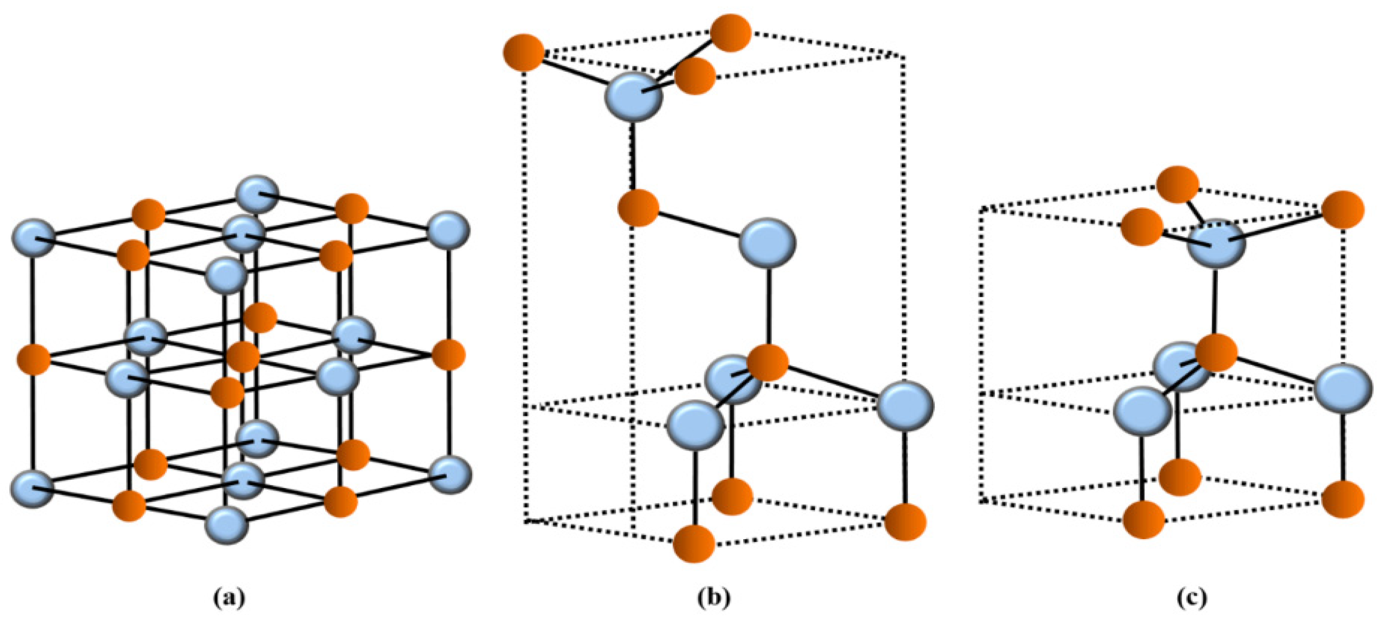
Figure 2.
Perturbation models for (a) an isolated ( symmetry) defect: The impurity atoms are occupying either the Zn atom on site (κ = 1) with neighboring host O atoms on sites 2, 3, 4, 5; or the O atom on site (κ = 2) with neighboring host Zn atoms on sites 1, 6, 7, 8 in ZnO. (b) Nearest-neighbor pair defect ( symmetry) where the two impurity atoms are occupying sites κ = 1 (Zn) and 2 (O), respectively. Impurity on Zn site has host O atoms at sites 3, 4, 5, while the impurity on O site has host Zn atoms at sites 6,7,8, respectively. (c) Second nearest-neighbor complex centers (/ symmetry) in the zinc-blend-type ZnO semiconductors. The complex can be formed by one impurity occupying Zn site at 1 and the other at site 6. If the two impurities are identical the symmetry is otherwise (see: text).
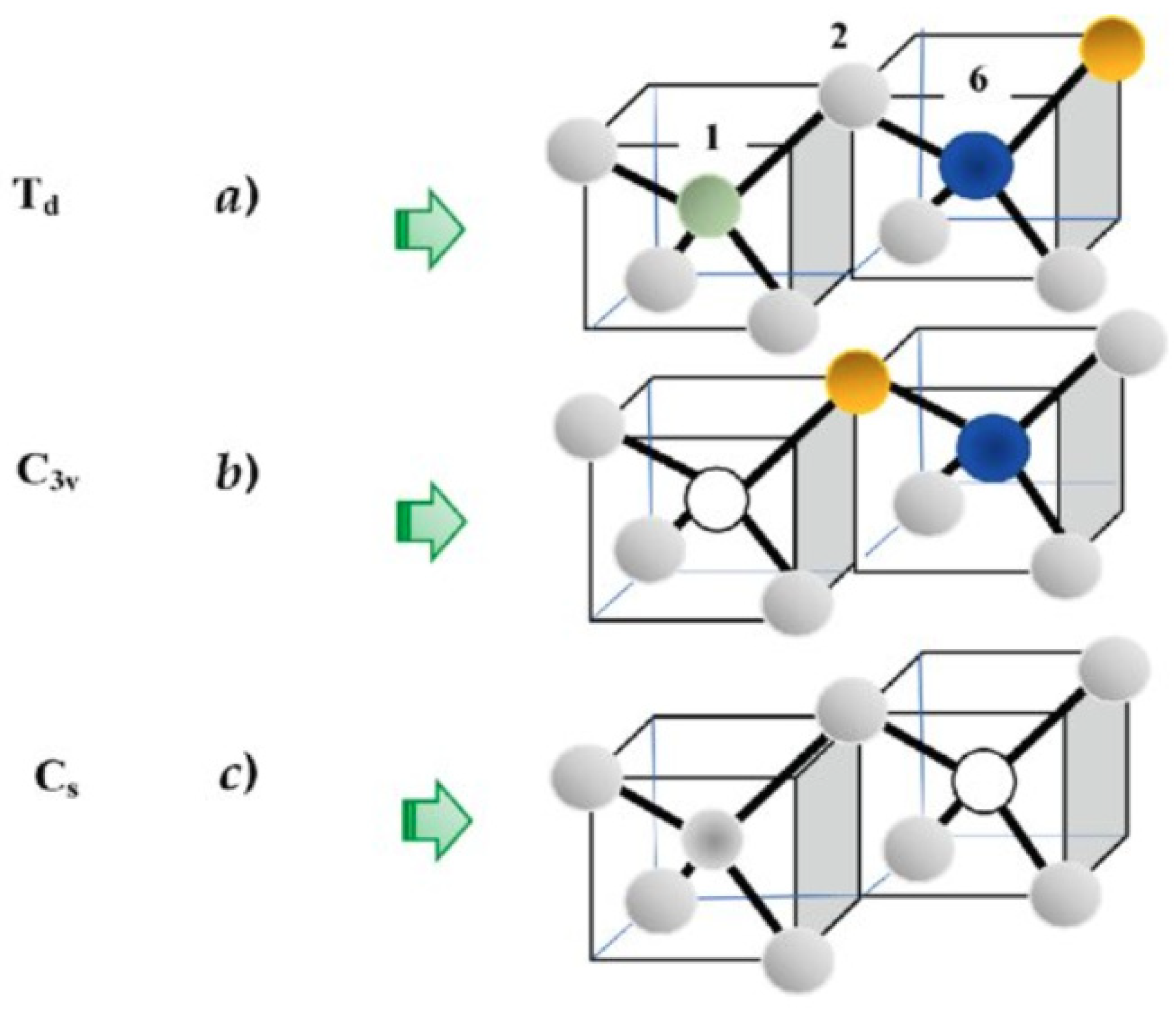
Figure 3.
The atomic displacements of optical phonon modes in the wz ZnO crystal structure. White colored spheres represent the Zn atoms while the red color spheres are indicated for the O atoms.
Figure 3.
The atomic displacements of optical phonon modes in the wz ZnO crystal structure. White colored spheres represent the Zn atoms while the red color spheres are indicated for the O atoms.
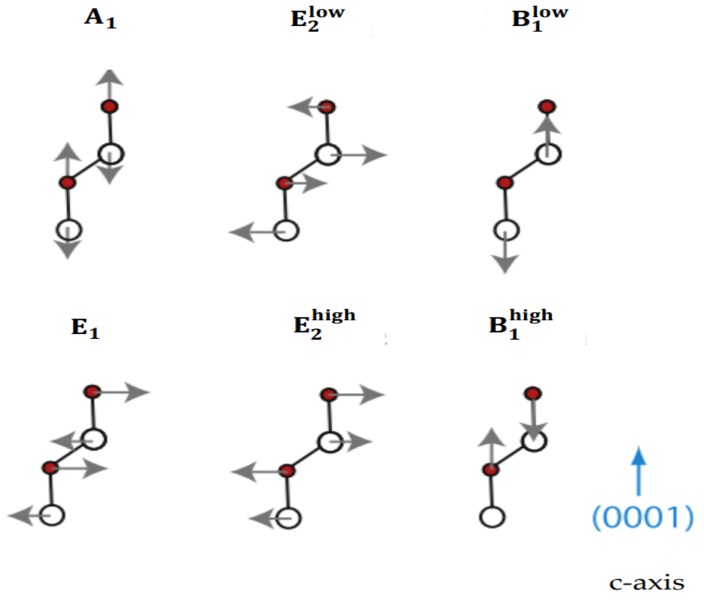
Figure 4.
(a) Rigid-ion-model calculations of the phonon dispersions for zinc blende ZnO material; (b) Rigid-ion-model calculations of the one phonon density of states exhibiting the phonon gap in zb ZnO occurring between the maximum acoustic modes and the minimum optical phonons region (shown by green colored vertical arrows) between ~275–405 cm−1.
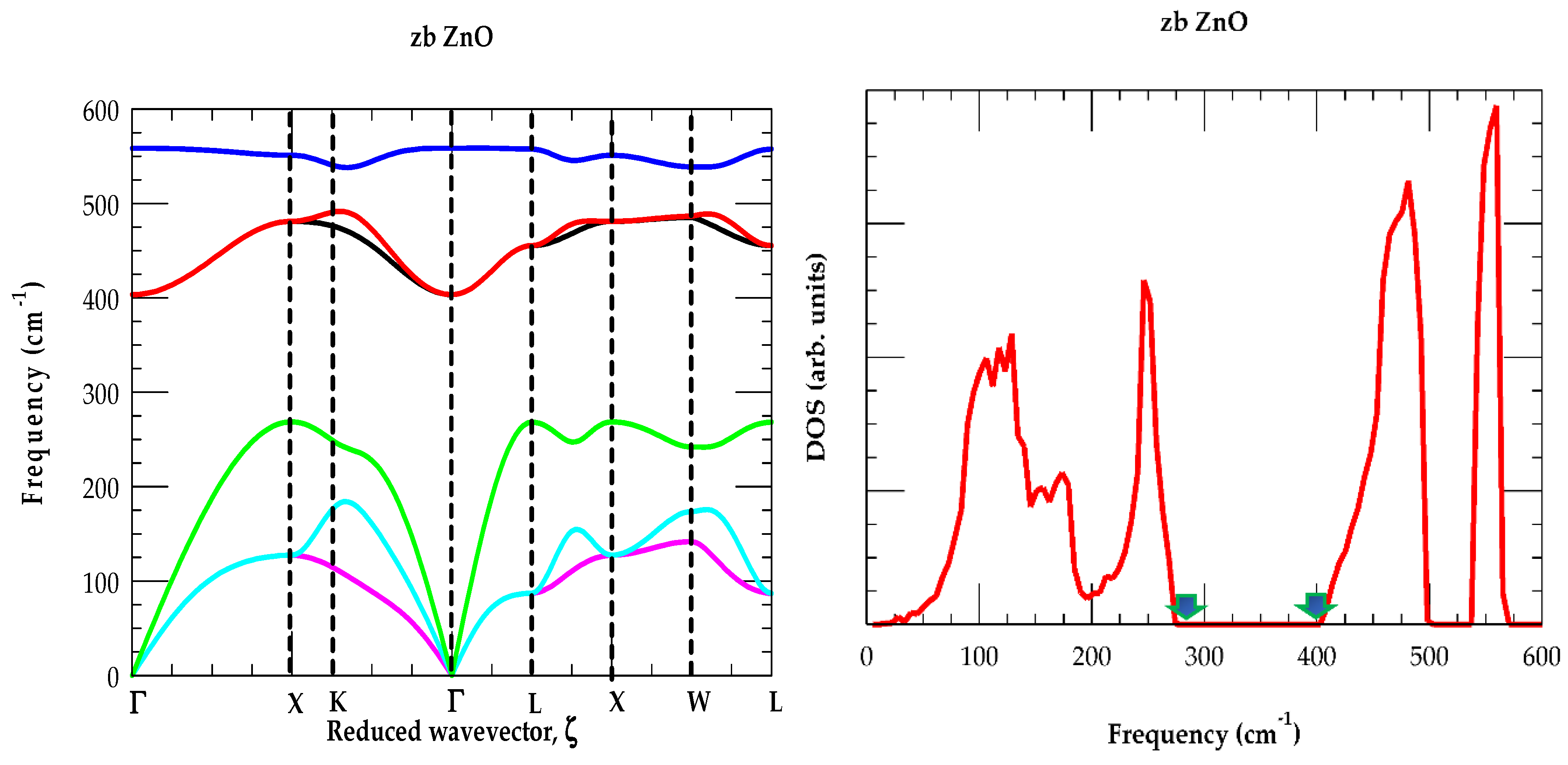
Figure 7.
Calculated real (black line) and imaginary (green line) parts of the det | I − GoP | (cf. Section 2.3.3) in the representation showing local and gap modes (see: Table 3) of (a) and (c) ZnO.
Figure 7.
Calculated real (black line) and imaginary (green line) parts of the det | I − GoP | (cf. Section 2.3.3) in the representation showing local and gap modes (see: Table 3) of (a) and (c) ZnO.
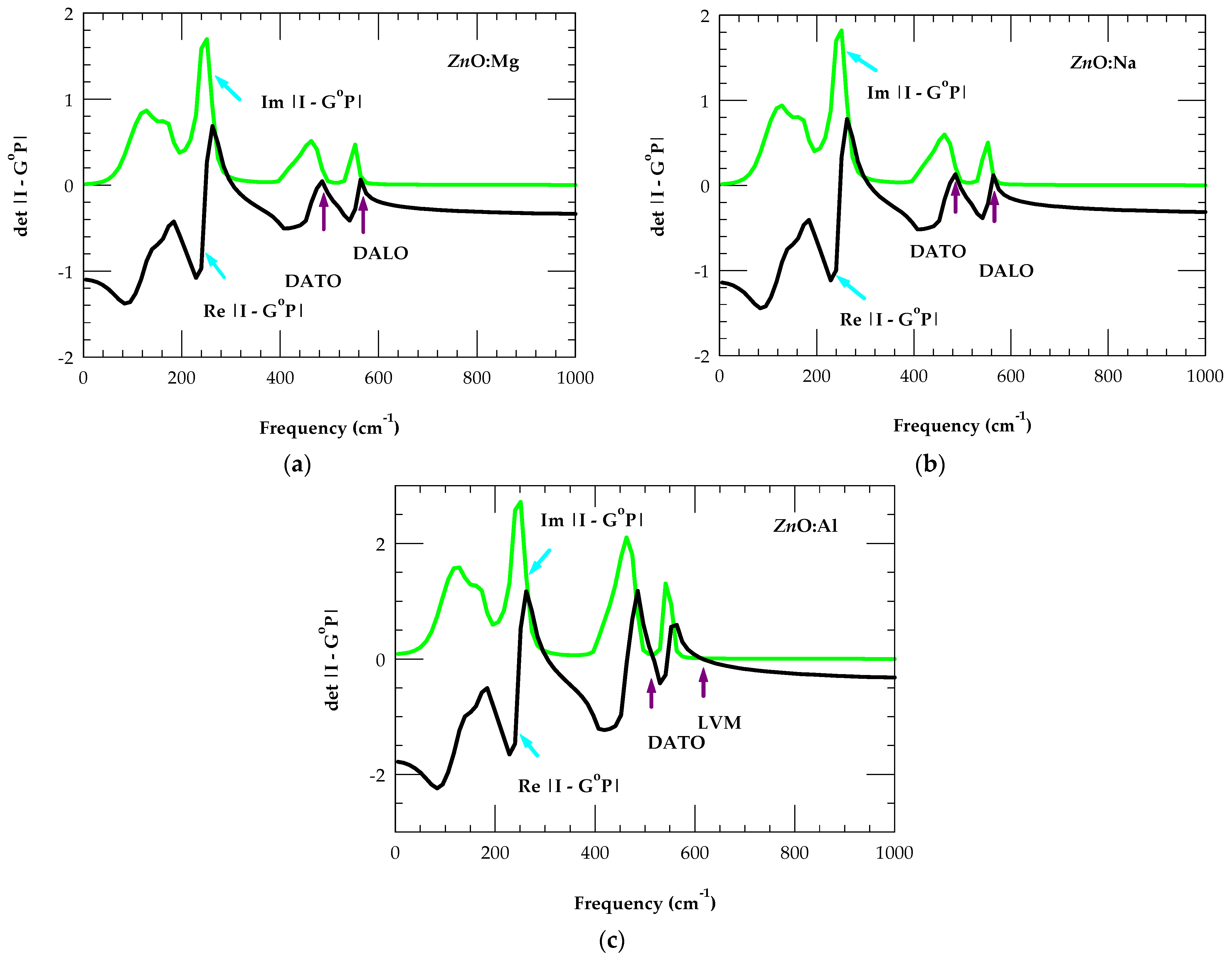

Table 1.
Comparison of major phonon frequencies in for the wz and zb ZnO.
| wz ZnO | zb ZnO | ||
|
|
560 (584, 575) 556 (595, 580, 588) 552 440 (438, 439) 409 (410, 411) 391 (380, 379) 261 91 (100) |
|
558 403 551 487 561 443 128 93 |
Table 2.
(i) Parameters required for optimizing the MREI model parameters Ref. [90] for calculating (ii) the two-mode behavior in ternary alloys.
Table 2.
(i) Parameters required for optimizing the MREI model parameters Ref. [90] for calculating (ii) the two-mode behavior in ternary alloys.
| (i) | |||||
|---|---|---|---|---|---|
| BeO | 728 | 1073 | BeO:Zn = 280 | 3.10 | 3.81 |
| ZnO | 403 | 558 | ZnO:Be = 775 | 5.32 | 4.504 |
|
θ |
3.10 5.32 2.99E+5 dyn/cm 2.40E+5 dyn/cm 5.96E+4 dyn/cm 0.12 |
||||
a) Ref. [90].
Table 3.
Comparison of GF calculations [of gap- (GMs), local vibrational- (LVMs) and in-band modes] with experimental data of the closest mass isoelectronic, acceptor and donor defects in ZnO.
Table 3.
Comparison of GF calculations [of gap- (GMs), local vibrational- (LVMs) and in-band modes] with experimental data of the closest mass isoelectronic, acceptor and donor defects in ZnO.
| System | Impurity-modes a) | Impurity modes (others)b) | Δf/f |
| ZnO:Li | 372 cm-1 (GM), 732 cm-1 (LVM) | 735 cm-1 | -0.17 |
| ZnO:Be | 363 cm-1 (GM), 775 cm-1 (LVM) | ~760, ~775 cm-1 | -0.50 |
| ZnO:B | 354 cm-1 (GM), 804 cm-1 (LVM) | 806, 819, 880 cm-1 | -0.82 |
| ZnO:Na | 305 cm-1 (GM), 486, 541 cm-1 | 270, 513 cm-1 | 0.07 |
| ZnO:Mg | 298 cm-1 (GM), 467, 551, 574 cm-1 | 250, 304, 490, 562, 568 cm-1 | -0.25 |
| ZnO:Al | 295 cm-1 (GM), 497, 545, 612 cm-1 | 475, 500, 560, 581, 623 cm-1 | -0.55 |
| ZnO:N | 497, 575 cm-1 | 277, 497, 512, 552, 575, 582 cm-1 | -0.1 |
| ZnO:P | 372 cm-1 (GM), 466, 543 cm-1 | 284, 361, 486 cm-1 | -0.14 |
| ZnO:As | 273, 470, 545 cm-1 | 220, 266, 550 cm-1 | -0.17 |
| ZnO:Sb | 235, 470, 545 cm-1 | 235, 534 cm-1 | -0.2 |
Table 4.
In zb ZnO, our predictions of localized vibrational modes using Greens function method for various complex defect centers of and symmetries.
Table 4.
In zb ZnO, our predictions of localized vibrational modes using Greens function method for various complex defect centers of and symmetries.
| zb ZnO | Modes (cm-1) | Average impurity mode | |
|
|
627 | -0.55 -0.10 |
|
|
616 602 |
611 | -0.55 -0.08 |
|
|
616 602 |
611 | -0.55 -0.06 |
|
|
616 602 |
611 | -0.55 -0.04 |
|
| : |
|
808 763 |
-0.83 -0.17 |
| : |
|
802 727 |
-0.83 -0.17 |
| : |
|
612 774 |
-0.55 -0.17 |
| : |
|
612 732 |
-0.55 -0.17 |
| : |
|
774 | -0.45 -0.17 |
| : |
|
737 | -0.45 -0.17 |
| : |
|
774 | -0.35 -0.17 |
| : |
|
730 | -0.35 -0.17 |
| : |
|
611 | 1.00 -0.55 |
| : |
|
797 |
1.00 -0.83 |
| : |
|
570 |
1.00 -0.1 |
Disclaimer/Publisher’s Note: The statements, opinions and data contained in all publications are solely those of the individual author(s) and contributor(s) and not of MDPI and/or the editor(s). MDPI and/or the editor(s) disclaim responsibility for any injury to people or property resulting from any ideas, methods, instructions or products referred to in the content. |
© 2025 by the authors. Licensee MDPI, Basel, Switzerland. This article is an open access article distributed under the terms and conditions of the Creative Commons Attribution (CC BY) license (http://creativecommons.org/licenses/by/4.0/).
Copyright: This open access article is published under a Creative Commons CC BY 4.0 license, which permit the free download, distribution, and reuse, provided that the author and preprint are cited in any reuse.


