Submitted:
23 December 2024
Posted:
25 December 2024
You are already at the latest version
Abstract
The effect of twin spacing and temperature on the mechanical behavior and deformation mechanism of nanotwinned AgPd alloy is investigated by molecular dynamics simulation. It is found that the nanotwinned AgPd alloy with small grain size shows a strengthening-softening transition with the reduction of twin spacing, which is attributed to the transition of dislocation from inclined to twin boundaries (TBs) to parallel to TBs. However, the nanotwinned AgPd alloy with large grain size shows a continuous strengthening with the decrease of twin spacing. It originates from the strain localization in grain boundaries and few dislocations are activated in the tensile processes. Lower temperatures increase the stability of preset twins and the formation of new twins, while higher temperatures promote atomic motion and migration of grain and twin boundaries, further exacerbating "detwinning."
Keywords:
Nanotwinned AgPd alloy
; Molecular dynamics simulation
; Twin spacing
; Temperature
; Deformation mechanism
1. Introduction
Nanotwinned metals with twin boundaries (TBs) inside ultrafine grains usually demonstrate an excellent combination of ultrahigh strength and good tensile ductility, compared to their twin-free nanocrystalline counterparts [1,2,3]. These excellent mechanical properties are associated with their unique deformation mechanism [4]. Thus, the mechanical behavior and deformation mechanism of nanotwinned metals have attracted extensive attentions in recent years.
Many experiments and theoretical studies have demonstrated that the classical Hall-Petch behavior of material strengthening with reduced twin spacing λ is broken below a critical spacing λc, that is the Hall-Petch breakdown or softening [5,6,7,8,9,10,11,12,13,14,15,16]. Lu et al. [5] synthesized different nanotwinned Cu samples with twin spacing varying from 94 nm down to 4 nm. The observations showed that its strength first increases as the twin spacing decreases, reaching a maximal strength at λ = 15 nm, then decreases as λ is further reduced. Molecular dynamics (MD) simulations [6] and theoretical calculations [7] showed that the strengthening-softening transition originates from the competition between dislocations inclined to TBs with those parallel to TBs, and the critical twin spacing λc depends on grain size d. Then Wei [8] further obtained the scaling law ∝ d1/2 based on the twin spacing-dependent plasticity model. Moreover, this strengthening-softening transition with the reduction of twin spacing has been observed in numerous metals and alloys [9,10,11,12,13,14,15,16].
In contrast, the unconventional continuous strengthening has been recently reported in some nanotwinned metals [17,18,19]. The experimental observation in columnar-grained nanotwinned Ni showed that the continuous strengthening can be extended to an extremely fine TB spacing [17]. The transmission electron microscopy (TEM) revealed that this continuous strengthening arises from the excellent stability of TBs and their strong impedance to dislocation motion. The continuous strengthening was also reported in nanotwinned (CoCrFeMn)1-xNix high-entropy alloys at Ni concentration below 44% [18], and it arises from the FCC-to-HCP martensite transformation. Furthermore, the MD simulation by Mousavi et al. [19] has shown that there exists a critical temperature in the nanotwinned Pd and Cu, below which the continuous strengthening occurs, while above which the strengthening-softening transition occurs. This continuous strengthening is driven by the stress concentration at the intersections of TBs and grain boundaries (GBs), which decreases with the reduction of twin spacing.
AgPd alloy is a widely used alloy in industries such as electronic communication, automotive and aviation, as well as new medical fields, with good corrosion resistance, conductivity, and high temperature resistance. The mechanical properties of materials are often closely related to their microstructure, and adding twinning to the material structure has become one of the ways to improve the comprehensive mechanical properties of materials. In this study, we investigate the effect of twin spacing and tenperature on the mechanical behavior and deformation mechanism of nanotwinned AgPd alloy by MD simulation. The paper is structured as follows: The methods of the model establishment and the simulation details are given in Section 2. The simulation results are discussed in Section 3 The conclusions are made in Section 4.
2. Computational Method
In order to systematically study the TB spacing and temperature deformation mechanism of nanotwinned AgPd alloys, equiaxed models with different TB spacing and average grain size were established. This section introduces the construction of the model, simulation details, and methods for analyzing simulation.
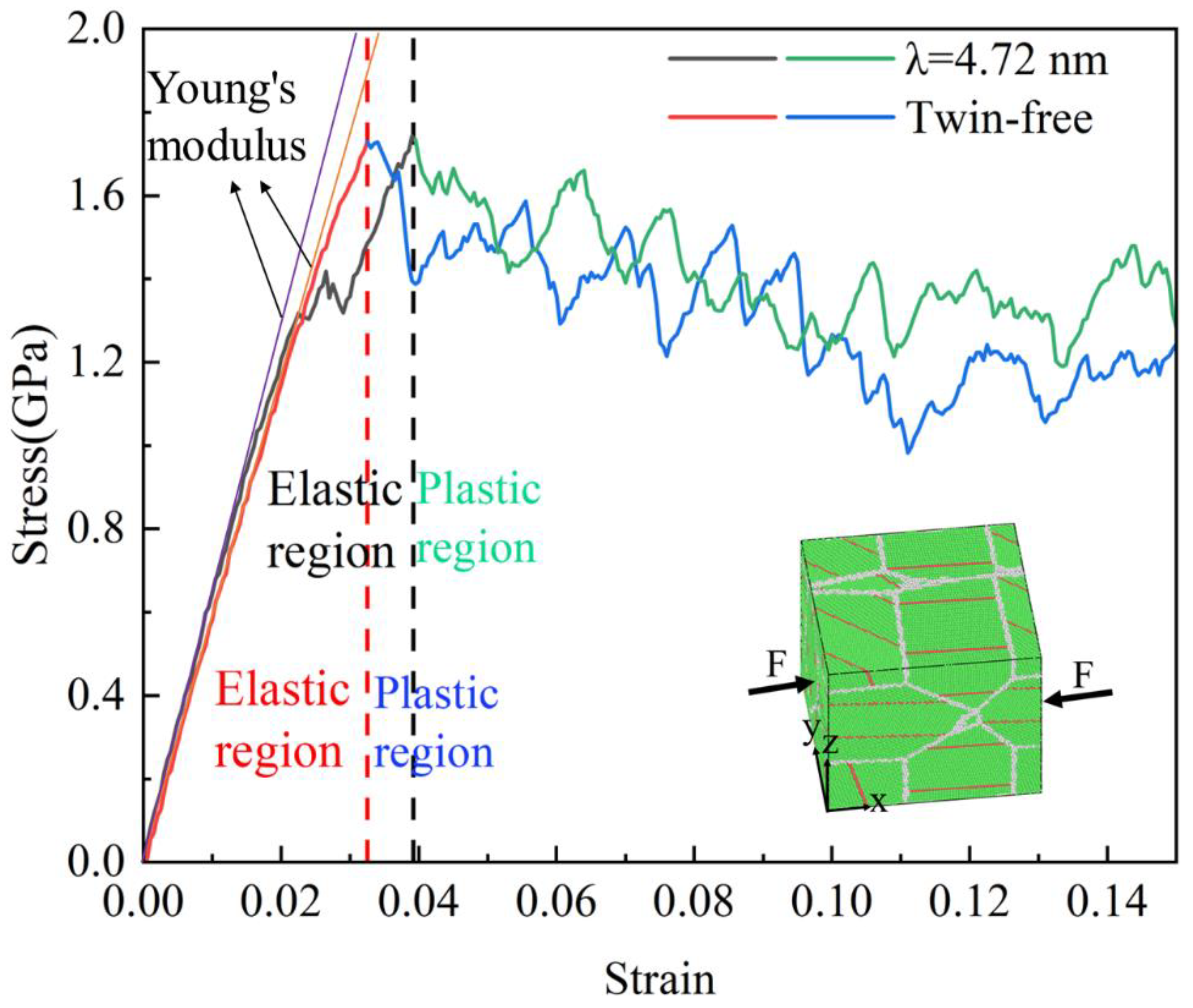
The Voronoi tessellation method embedded in Atomsk [20] was used to generate polycrystalline silver palladium alloy model. The twin-free and twin-containing equiaxed-grained samples with specific atomic ratios were constructed according to the methods of Hua et al. [21] and Yan et al. [22]. To obtain the simulation model for the twin-free equiaxed-grained Ag0.5Pd0.5 samples, the equiaxed-grained pure Pd models were established at first, then the Pd atoms in the pure Pd models were randomly replaced with Ag to obtain the target composition. For the equiaxed-grain Ag0.5Pd0.5 sample with different TB spacings, the nanotwinned Pd models were first established and then the atoms were randomly replaced in a similar way as used for twin-free Ag0.5Pd0.5 alloy models to get the target atoms ratio. Fig 1 shows the stress-strain curve of a silver palladium nanoalloy with an average grain size of 11.00 nm. Compared to the nano polycrystalline silver palladium alloy without twinning structure, the alloy with twinning has differences in elastic-plastic transformation and average flow stress, lagging behind the elastic-plastic transformation and increasing the average flow stress. Table 1 provides the initial configuration related parameters for model sizes of 25 nm × 25 nm × 25 nm, 20 nm × 20 nm × 20 nm, 15 nm × 15 nm × 15 nm, 10 nm × 10 nm × 10 nm, respectively. In the sample with grain size d = 5.50 nm, the largest twin spacing is λ = 4.04 nm due to the small grain size.
The large-scale atomistic/molecular massively parallel simulator (LAMMPS) [23] is used for conducting MD simulation. The motion equations are solved by velocity-Verlet [24] algorithm with a time step of 1 fs. The accuracy and reliability of MD simulation results are dependent on the utilized interatomic potential. The embedded atom model (EAM) potential developed by Hale et al. [25] is used to describe the interaction between atoms in nanotwin AgPd alloy, and the interatomic interaction potential can is given as the following
Here, EC is the cohesive energy, N is the total number of atoms, is the atomic spacing between atoms i and j, is the embedding energy function for atom i, is the electron density function for atom j and is the pair interaction function between atoms i and j. is the total electron density felt by atom i from all other atoms j. EAM places no limitations on the exact mathematical expressions used for the three functions F, ρ and , but practice and theory point to particular characteristic forms for each. It can correctly reflect the thermodynamic, dynamics and microstructural properties of AgPd alloy system.
Figure 1.
Stress-strain curve of silver palladium nanoalloy with an average grain size of 11.00nm.
At the beginning of simulation, each initial configuration is isothermally relaxed for 50 ps at 300 K to obtain equilibrium configurations using Nose–Hoover thermostat [26,27]. Subsequently, these nanotwinned samples are axially loaded at a strain rate of 1.0 × 10⁸ s-1 along the x-axis at 300 K. Periodic boundary conditions are imposed along three coordinate axes. In order to study the effect of temperature on the deformation behavior of nanocrystalline polycrystalline AgPd alloys with different twin spacing, a configuration with an average grain size of 11.00 nm was selected, and the selected temperatures were 10 K, 100 K, 300 K, and 500 K. Set the relaxation temperature at 10 K, 100 K, 300 K, and 500 K to relax for 50 ps and load at the corresponding temperature, with a strain rate of 5.0 × 10⁸ s-1.
The free Open Visualization Tool (OVITO) [28] was used to analyze the simulation results. The CNA module and DXA module in OVITO were employed to visualize the atomic configuration. In this study, atoms were colored based on CNA: green for FCC atoms, red for hexagonal close-packed (HCP) atoms, blue for body-centered cubic (BCC) atoms, and white for unknown atoms. In OVTIO analysis, one layer of HCP structure atomic plane represents twin boundary (TB), two adjacent HCP structure atomic planes represent intrinsic stacking fault (ISF), and there is an FCC structure atomic plane between the two HCP structure atomic planes representing extrinsic stacking fault (ESF), with three or more HCP structure atomic planes representing HCP phase. Blue, green, magenta, yellow, and light blue lines represent all dislocation lines, Shockley, Stair rod, Hirth, and Frank dislocation lines, respectively.
3. Results and Discussion
3.1. Effect of Twin Spacing on the Mechanical Behavior of Nanotwin AgPd Alloy
In order to clarify and avoid interference, the chapter does not discuss chemical composition factors, and AgPd is generally assumed to be composed of 50% silver and 50% palladium. According to previous experiments and simulation calculations, the stacking fault energy range of AgPd is 16-180 mJ/m2, with Ag0.5Pd0.5 being 60 mJ/m2, which belongs to alloys with lower stacking fault energy. Figure 2 shows the stress-strain curves of AgPd alloy with average grain sizes of 5.50 nm, 8.24 nm, 11.00 nm, and 13.76 nm under different twin spacing during compression. At the beginning, the curve rapidly increases when the strain rate is small, corresponding to the elastic deformation stage of the alloy deformation stage. Then, with the increase of external load, it enters the plastic deformation stage, and the curve stabilizes and fluctuates. For the nanotwin configuration with an average grain size of 5.50 nm, due to the high proportion of disordered structural atoms in the model, the curve fluctuates greatly, and the slope of the rising curve is slower than that of larger sizes. Due to considerations for the accuracy of simulation results and computational resources, it has been decided to use the nanotwin configuration at a model size of 20 nm x 20 nm x 20 nm as a study to investigate the influence of twin spacing and other factors.
Figure 3 shows the average flow stress variation curves of AgPd alloy with average grain sizes of 5.50nm, 8.24nm, 11.00nm, and 13.76nm at different twin spacing during compression. In nanotwin configurations with smaller grain sizes (average grain sizes of 5.50 nm, 8.24 nm, 11.00 nm), as the twin spacing increases from 0.67 nm, the average flow stress first increases and then begins to decrease with the increase of twin spacing; However, for nanotwin configurations with larger grain sizes (average grain size of 13.76 nm), the average flow stress gradually decreases with the increase of twin spacing, and the twin spacing at 0.67 nm reaches its maximum value. Similarly, the average flow stress of the nano polycrystalline configuration without twin structure is lower than that of the configuration with twin structure, indicating that the mechanical properties of the silver palladium nano alloy with added twin structure have improved.

Table 2.
Statistical analysis of mechanical properties of nanotwin AgPd alloy with average grain sizes of 11.00nm and 13.76nm.
Table 2.
Statistical analysis of mechanical properties of nanotwin AgPd alloy with average grain sizes of 11.00nm and 13.76nm.
| Average grain size (d/nm) |
Twin spacing (λ/nm) |
Young's modulus (GPa) | Yield strength (GPa) | Average flow stress (GPa) | Elastic-plastic strain transition value |
| 11.00 | 0.67 | 56.07 | 1.49 | 1.21 | 0.029 |
| 1.35 | 61.97 | 1.68 | 1.50 | 0.028 | |
| 2.02 | 61.84 | 1.84 | 1.41 | 0.038 | |
| 3.37 | 62.52 | 1.85 | 1.34 | 0.041 | |
| 4.72 | 63.24 | 1.86 | 1.35 | 0.039 | |
| 6.74 | 62.31 | 1.79 | 1.34 | 0.040 | |
| twin-free | 62.52 | 2.02 | 1.17 | 0.033 | |
| 13.76 | 0.67 | 54.22 | 1.45 | 1.51 | 0.041 |
| 1.35 | 61.06 | 1.57 | 1.39 | 0.047 | |
| 2.02 | 61.00 | 1.50 | 1.33 | 0.040 | |
| 3.37 | 58.08 | 1.54 | 1.34 | 0.043 | |
| 4.72 | 57.24 | 1.50 | 1.25 | 0.041 | |
| 6.74 | 61.46 | 1.49 | 1.21 | 0.039 | |
| twin-free | 67.62 | 2.06 | 1.20 | 0.036 |
3.2. Effect of Twin Spacing on the Deformation Mechanism of Nanotwin AgPd Alloy
For nanotwin AgPd configurations with a size of 20 nm x 20 nm x 20 nm, the model reached a stable state after 50 ps relaxation. Before deformation, the atomic proportions of each structural atom in different twin spacing configurations are shown in Figure 4. The proportion of HCP structural atoms to a certain extent reflects the density of twin structures in the configuration. As the twin spacing increases, the proportion of HCP structural atoms gradually decreases, while the proportion of FCC structural atoms gradually increases. BCC and other structural atoms remain basically unchanged. Figure 5 shows the atomic variation and stress variation trend with strain of nanotwin AgPd alloys with different twin spacing. In the early stage of strain, the number of atoms with four different structures does not change much, corresponding to the plastic deformation stage of the stress-strain curve. At this time, the stress value is small and not enough to cause the atomic structure to undergo transformation. When the stress value increases to the yield limit, the number of structural atoms begins to change significantly. For the configuration with the smallest twin spacing, that is λ= 0.67 nm, the number of HCP structural atoms began to continuously decrease, while the number of FCC structural atoms continued to increase, and other disordered structural atoms also slowly increased, indicating that during the deformation process of high twin density configurations, some HCP structural atoms transformed into FCC and other disordered structural atoms; For configurations with twin spacing of 2.02 nm, 3.37 nm, 4.72 nm, and 6.74 nm, the number of HCP structural atoms continues to increase, while the number of FCC structural atoms continues to decrease. In the later stage of stress-strain curve fluctuation, the changes of the two become slower, while there are decreases or increases in other disordered structural atoms before and after deformation, but the amount of change is not significant; For the configuration with a twin spacing of 1.35 nm, the difference is that the increase in HCP structure atoms is not significant before and after deformation, while other disordered structure atoms continue to increase, FCC structure atoms continue to decrease, and the change slows down in the later stage of deformation. Based on this characteristic and combined with the configuration where the average flow stress value is higher than other twin spacing, the study of temperature on the deformation behavior and mechanism of AgPd alloy nanocrystals at 1.35 nm is reasonable and representative.
Figure 6 shows the variation of various types of dislocation line lengths with strain during the deformation process of nanotwin AgPd alloys with different twin spacing. During the deformation process, the initial deformation stage is similar to the CNA structure, with less variation in the length of various dislocation lines, mainly Shockley dislocations and Perfect dislocations, and a small proportion of Stair rod, Hirth, and Frank dislocations. As the strain continues, some of the Shockley dislocations rapidly increase and become the main dislocations, while the Perfect dislocations change very slowly. Among different twin spacing, the maximum difference in dislocation line length between Shockley before and after deformation is 0.67 nm, and the maximum dislocation line length before and after deformation is 6.74 nm. In order to better describe the deformation process characteristics from the perspective of dislocations, all types of dislocation lines were statistically analyzed and the dislocation density variation process of nanotwin AgPd alloy with different twin spacing was calculated, as shown in Figure 7. Among the six types of twinning spacing, the twinning spacing at 1.35 nm has the lowest total dislocation density, while the twinning spacing at 6.74 nm has the highest total dislocation density and the smallest difference before and after, indicating that there is less dislocation generation during its deformation process.
In order to better analyze the influence of different twin spacing, the characteristics of the stress-strain curve and various structural atomic change curves in Fig 5 were combined, and before external loading, i.e. after relaxation, were selected; The four states in the stress-strain curve, including elastic limit, stable and slow change of HCP structure atoms in the middle stage of deformation, and completion of strain, were selected. Three sets of twinning spacing, 0.67 nm, 1.35 nm, and 6.74 nm, were selected to compare and analyze the various dislocations and microstructures that occur during the deformation process of the nanotwin AgPd alloy. At the same time, the deformation process without twinning configuration under the same deformation conditions was selected as the control, Observe the effect of twin structure on the stability of material structure. Figure 8 shows the atomic diagram of the compression process of a nano polycrystalline AgPd alloy with an average grain size of 11.00 nm and no twinning structure. In the stage of elastic deformation, structural defects first appear at the grain boundary due to stress concentration, and some of the atoms near the grain boundary transform into HCP structural atoms, providing a prerequisite for subsequent dislocation source emission, as shown in Fig (a); After the stress value exceeds the yield stress, a large number of dislocations are emitted from grain boundaries and intragranular defects, resulting in some free dislocations and stacking fault structures. Under the obstruction of grain boundaries, the growth of dislocation line length and dislocation density slows down, and some stacking fault structures transform into twin structures, as shown in Fig (d). During the entire deformation process of nano polycrystalline AgPd alloy without twin structure, dislocation stacking and twin structure occur successively, which interact with each other and cause changes and fluctuations in material stress. Among them, grains I and III are severely damaged before and after deformation, indicating that the movement of grains and dislocations plays an important role in nano polycrystalline materials.
Figure 9 shows the atomic diagram of the compression process of a nanocrystalline polycrystalline AgPd alloy with a twin spacing of 0.67 nm and an average grain size of 11.00 nm. After relaxation, FCC structure atoms appeared between twin boundaries in grain I and transformed into other disordered structure atoms, indicating the presence of certain stresses at the grain; After the strain reaches the elastic limit, dislocations begin to proliferate and expand, mainly Shockley partial dislocations. Dislocations interact with pre-existing twins, which hinder the expansion of dislocations. Dislocations cause an increase in stress values at twin boundaries, and multiple HCP atoms at twin boundaries transform into disordered atoms, indicating that the sample begins to undergo de twinning phenomenon. During the middle and later stages of strain, the twin boundaries in grains I and II shift, resulting in a decrease in twin spacing or even breakage of twin boundaries. Some stacking fault structures containing intrinsic and extrinsic stacking faults appear, but in grain III, where the twin boundary direction is almost perpendicular to the loading direction, except for a small amount of twin structures that undergo de twinning, most twin structures are not damaged throughout the loading process, Even if the twin spacing and applied strain are the same, the different angles between the pre-existing twin boundaries and the loading direction will trigger different deformation mechanisms. Based on the shear strain diagram and displacement vector diagram of the corresponding strain state, it can be seen that stress is mainly concentrated at grain boundaries and interlayer dislocations, with stress concentration observed at a few twin boundaries. The relative displacement of atoms at grain boundaries is significantly higher than that at twin boundaries and within grains. For twin boundaries with relatively concentrated stress in the middle and later stages of deformation, their displacement vector values are also correspondingly high.
Figure 10 shows the atomic diagram of the compression process of a nanocrystalline polycrystalline AgPd alloy with a twin spacing of 1.34 nm and an average grain size of 11.00 nm. After relaxation, the structure at the twin boundaries did not undergo any transformation, only some disordered structural atoms at the grain boundaries transformed into HCP structural atoms; After the stress reaches the elastic limit, some Shockley dislocations are emitted at the grain boundary of grain I. During the slip process of dislocations, they are blocked by the existing twin grain boundaries, ultimately causing the twin boundaries to migrate to one side, resulting in a change in the twin spacing; In the middle and later stages of deformation, some twin boundaries near the grain boundary undergo "de twinning" phenomenon. Combined with the shear strain diagram (c1), the strain is more severe here. Some twins are impacted by the movement of dislocations at the grain boundary, and dislocations accumulate and penetrate the twin boundary, ultimately resulting in changes in twinning spacing or twinning structure annihilation. In addition, due to the movement of dislocations, twinning originally existing at the grain boundary II later produces an ISF structure, Finally, the grain is compressed and meets the twin boundaries. For the displacement vector diagram of this process, most of the displacement vector values at grain boundaries and within grain II are high, indicating that grain boundaries and twin boundaries are hindering dislocation movement while also undergoing migration and variation. Figure 11 shows the atomic diagram of the compression process of a nanocrystalline polycrystalline AgPd alloy with a twin spacing of 6.74 nm and an average grain size of 11.00 nm. After the stress reaches the elastic limit, the two Shockley partial dislocations at the grain boundary and inside the grain act on the same twin, causing it to eventually divide into several intermittent twin and layer fault structures. In the later stage of deformation, some new twin structures and V-shaped secondary twin structures were generated, as shown in Fig (d). The black dashed box shows the upcoming secondary twin structures.
3.3. Effect of Temperature on the Mechanical Behavior of Nanotwin AgPd Alloy
Some researchers believe that as the temperature of the system increases, the energy obtained by atoms will increase, leading to an increase in their vibration frequency and amplitude, making it easier to move across obstacles such as grain boundaries, phase boundaries, and solute clusters. Therefore, as the temperature increases, the movement of dislocations and grain boundaries, as well as the diffusion of atoms, become easier. In order to study the effect of temperature on the deformation behavior of nanocrystalline polycrystalline AgPd alloys with different twin spacing, referring to the deformation characteristics of different size configurations in Table 1 and Figure 2, a configuration with an average grain size of 11.00 nm was selected.
Figure 12 shows the stress-strain curves of nanotwin AgPd alloy after relaxation at 10 K, 100 K, 300 K, and 500 K temperatures and compression at the same temperature. At different temperatures, the stress-strain curve shows a rapid increase in stress at the beginning of the strain, followed by a decrease at a certain value and then a stable fluctuation. It is worth noting that the parameters during the strain process change when the temperature changes. For example, for the same twinning spacing, the elastic modulus and elastic limit increase with the decrease of temperature. Figs 13 show the variation curves of Young's modulus and average flow stress of nanotwin AgPd alloy under compression at different temperatures, as the twin spacing decreases. As the temperature decreases, the Young's modulus and average flow stress corresponding to different twin spacing increase. For the same temperature, the Young's modulus basically increases with the increase of twin spacing. When the twin spacing is 0.67 nm, the Young's modulus decreases more. As the twin spacing decreases, the average flow stress at any temperature shows a trend of first increasing and then decreasing. However, the twinning spacing corresponding to the turning point is different, with 1.35 nm for 100 K and 500 K, and 2.02 nm and 3.37 nm for 300 K and 10 K, respectively.
Table 3.
Statistical analysis of mechanical properties related to deformation of nanotwin AgPd alloy with an average grain size of 11.00nm at different temperatures.
Table 3.
Statistical analysis of mechanical properties related to deformation of nanotwin AgPd alloy with an average grain size of 11.00nm at different temperatures.
| Deformation temperature (T/K) |
Twin spacing (λ/nm) |
Young's modulus (GPa) | Yield strength (GPa) | Average flow stress (GPa) | Elastic-plastic strain transition value |
| 10 | 0.67 | 65.25 | 1.72 | 1.59 | 0.031 |
| 1.35 | 71.70 | 2.00 | 1.81 | 0.034 | |
| 2.02 | 73.83 | 2.18 | 1.80 | 0.042 | |
| 3.37 | 71.83 | 2.13 | 1.86 | 0.041 | |
| 4.72 | 71.53 | 2.28 | 1.80 | 0.045 | |
| 6.74 | 73.29 | 1.96 | 1.82 | 0.043 | |
| 100 | 0.67 | 61.00 | 1.72 | 1.54 | 0.038 |
| 1.35 | 68.78 | 1.95 | 1.75 | 0.039 | |
| 2.02 | 68.27 | 1.99 | 1.76 | 0.047 | |
| 3.37 | 68.39 | 2.12 | 1.66 | 0.042 | |
| 4.72 | 68.68 | 2.18 | 1.62 | 0.048 | |
| 6.74 | 69356 | 1.96 | 1.58 | 0.045 | |
| 300 | 0.67 | 61.00 | 1.49 | 1.27 | 0.033 |
| 1.35 | 61.97 | 1.68 | 1.48 | 0.031 | |
| 2.02 | 61.84 | 1.84 | 1.55 | 0.041 | |
| 3.37 | 62.52 | 1.85 | 1.52 | 0.042 | |
| 4.72 | 63.24 | 1.86 | 1.44 | 0.042 | |
| 6.74 | 62.31 | 1.79 | 1.38 | 0.048 | |
| 500 | 0.67 | 48.78 | 1.23 | 1.11 | 0.035 |
| 1.35 | 49.49 | 1.41 | 1.30 | 0.036 | |
| 2.02 | 50.91 | 1.62 | 1.30 | 0.045 | |
| 3.37 | 49.02 | 1.60 | 1.24 | 0.045 | |
| 4.72 | 53.31 | 1.48 | 1.21 | 0.043 | |
| 6.74 | 52.42 | 1.43 | 1.24 | 0.042 |
3.4. Effect of Temperature on the Deformation Mechanism of Nanotwin AgPd Alloy
Figure 14 shows a comparative analysis of the atomic proportions of various structures in AgPd alloys with twin spacing of 1.34nm after relaxation at different temperatures. As the relaxation temperature increases, the number of FCC and HCP structural atoms decreases, but the number of HCP structural atoms changes less; The number of atoms in the Other structure increases accordingly. After the temperature increases, the energy obtained by some atoms in the configuration increases, leading to a transition from FCC and HCP structured atoms to Other structured atoms, resulting in an increase in the proportion of disordered structured atoms in the configuration. Figure 15 shows the trend of atomic changes and stress with strain during the deformation process of AgPd alloy with twin spacing of 1.34 nm at temperatures of 10 K, 100 K, 300 K, and 500 K. When the deformation temperature is low, as shown in Figs. 15 (a) 10 K and (b) 100 K, in the initial stage of strain, the FCC structural atoms begin to gradually decrease, while the Other structural atoms begin to increase. At this time, the HCP structural atoms remain basically unchanged; When the stress value exceeds the elastic limit and yield upper limit, the number of HCP structural atoms begins to increase. This process is mainly due to the transition of FCC structural atoms to HCP and Other structural atoms, indicating that the stress value is relatively small in the early deformation stage and the HCP structural atoms are relatively stable in the configuration; As the stress value increases in the later stage, the strain increases, and the stress concentration in the grains is more severe. The HCP structural atoms in twinning and stacking fault structures begin to change. When the deformation temperature is high, as shown in Figure 15 (d) 500 K, in the initial stage of deformation, the number of various structural atoms remains basically unchanged. When the stress value increases to the elastic limit, the number of HCP and FCC structural atoms begins to decrease, and the number of Other structural atoms begins to increase, indicating that there is a transition from HCP and FCC structural atoms to Other structural atoms at this stage. It can be seen that the decrease in temperature to some extent increases the stability of the twin structure.
Figure 16 shows the variation trend of the length of various types of dislocation lines with strain in AgPd alloy with twin spacing of 1.34 nm at different deformation temperatures. During the entire deformation process, Shockley dislocations accounted for the vast majority, followed by Perfect dislocations, while Stair rod, Hirth, and Frank dislocations accounted for very little, almost zero. The length of various dislocation lines after relaxation at 10 K, 100 K, and 300 K is basically not affected by temperature, and there is not much difference between them; However, after relaxation at 500 K temperature, the length of various dislocation lines is less compared to other temperatures, indicating that the extension of dislocations is less after temperature increase. Based on the trend chart of the total dislocation density of the alloy with strain at different temperatures, as shown in Figure 17, during the entire deformation process, increasing the deformation temperature results in a decrease in the corresponding total dislocation density, indicating that temperature has a certain inhibitory effect on the generation of defects such as dislocations and stacking faults.
In order to better compare the influence mechanism of temperature on the nanotwin AgPd alloy, combined with the characteristics of the configuration stress-strain curve and the CNA structure number change curve, four stages were selected: relaxation without deformation, strain reaching the elastic limit, FCC structure atom reduction to stable stage, and deformation completion. The evolution characteristics of dislocations and microstructures with a twin spacing of 1.42 nm configuration at 10 K, 300 K, and 500 K temperatures were analyzed, As shown in Figs 18. When the temperature is low (T=10K), after relaxation, some HCP and BCC structural atoms appear at the grain boundaries, with a higher proportion compared to other temperatures; Deformation reaches the elastic limit, and twinning dislocations sprout at the black dashed line of grain I and move in the direction of the arrow in the Fig, causing the twinning to move away from adjacent twinning towards the grain boundary; As deformation continues, twinning in grains II and IV is severely damaged, resulting in the formation of ISF and ESF structures. It is worth noting that the transformation process from ESF to ISF structure has been observed, with some exhibiting ESF structure and the other exhibiting ISF structure, and new twinning appears at the junction of these two grains. Although the twinning length here is not long due to the obstruction effect of grain boundaries, it alleviates the degree of stress concentration here; After deformation to 15%, the black solid line of grain III has transformed into a shorter ISF structure, and new twinning has appeared at the grain boundary. When the temperature is high (T=500K), after relaxation is completed, a certain amount of FCC and HCP structural atoms appear between the grain boundaries and within the grains, transforming into other disordered structural atoms. These defects provide nucleation points for dislocation germination to a certain extent. Compared to low temperatures, the small grains at the grain boundaries marked by the yellow circle temporarily disappear during the relaxation process and gradually appear again during subsequent deformation, indicating that higher temperatures promote the activity of grain boundaries. Deformation reaches the elastic limit, and the transformation of disordered structures within the grain increases. Dislocation sources appear at the twin boundaries within grain II and further move towards the grain boundaries, ultimately leading to a decrease in twin spacing and partial twinning annihilation. When the deformation reaches 10.00%, the number of atoms in the FCC structure enters a slow fluctuation stage. At this stage, ESF structures appear near the grain boundaries of grain II, and the twinning spacing within other grains decreases to varying degrees. After deformation, the grain boundaries within grains II and IV were severely damaged, and twinning within grain II almost disappeared. Large disordered atomic clusters appeared within grain IV.
In order to determine the degree of influence of temperature factors on the average flow stress of AgPd alloy with twin spacing of 0.67 nm at room temperature of 300 K, which is lower than other twin spacing, the deformation process of this twin spacing was selected at temperatures of 10 K and 500 K. Figure 19 shows the atomic diagram of the nanocrystalline polycrystalline AgPd alloy with a twin spacing of 0.67 nm and an average grain size of 11.00 nm during 10 K compression. After relaxation, the twin structure and intra crystal atoms did not change. After strain reached the elastic limit, the phenomenon of "de twinning" appeared in grain I. The reason was that the dislocations emitted at the grain boundary met with the twin here, forcing the twin boundary to migrate towards the direction of dislocation movement, as shown in Fig (b); When the strain reached 13.05%, the twin structure inside grain III basically annihilated and transformed into structures such as ISF and ESF. After the strain was completed, the ISF structure shown in the black box also disappeared. For AgPd alloys with the same parameters compressed at a temperature of 500 K, as shown in Figure 20. After relaxation, some atoms in the twin boundaries and grains transform into disordered structural atoms, providing a location for subsequent dislocation source emission. After reaching the elastic limit, the phenomenon of "de twinning" occurs in grain III. In the later stage of deformation, the twin structure also transforms into an ESF structure, resulting in a decrease in the number of twin structures. By analyzing the changes in the density of various structural atoms and dislocations at two different temperatures, it was found that there was not much difference in the reduction of HCP structural atoms. However, at 500 K, the main transition occurred from HCP structural atoms to disordered structural atoms, while at 10 K, the transition occurred to FCC and disordered structural atoms. Higher temperatures to some extent intensified the trend of atomic motion. This exacerbates the annihilation of twin structures.
4. Conclusions
This paper simulates the compression deformation process of nanocrystalline polycrystalline AgPd alloys with different twin spacing using molecular dynamics methods, and explores the effects of twin spacing, deformation temperature, and strain rate on the mechanical properties and deformation mechanism of AgPd alloys during deformation. The results show that:
(1) The average flow stress of nanotwin AgPd alloys with average grain sizes of 5.50 nm, 8.24 nm, and 11.00 nm increases first and then decreases with the decrease of twinning spacing. Among them, the alloy with average grain size of 11.00 nm increases and then decreases with the decrease of twinning spacing λ= The average flow stress at 1.35 nm reaches its maximum value; The average flow stress of the nanotwin AgPd alloy with an average grain size of 13.76 nm continued to increase with the decrease of twin spacing, and there was no turning trend. The average flow stress of nanocrystalline polycrystalline AgPd alloy with added twin structure is higher than that without twin structure. During the deformation process of a nanotwin AgPd alloy with an average grain size of 11.00 nm, the alloy with a twin spacing of 0.67 nm experiences a phenomenon of "de twinning"; The alloy with a twin spacing of 6.74 nm exhibits new twin structures and V-shaped secondary twinning.
(2) By changing the relaxation temperature and deformation temperature of the nanotwin AgPd alloy with an average grain size of 11.00 nm, it was found that as the temperature increased, the Young's modulus and average flow stress of the nanotwin AgPd alloy gradually decreased; On the microstructure, it was found that the AgPd alloy with a twin spacing of 1.35 nm transformed from HCP and FCC structural atoms to Other structural atoms at higher temperatures (500 K), and from FCC structural atoms to HCP and Other structural atoms at lower temperatures (10K and 100K). The length and total dislocation density of the Shockley dislocation lines, which occupy the main position in the dislocation lines, increased with decreasing temperature. Lower temperatures will increase the stability of preset twins and the generation of new twins, while higher temperatures will promote the movement of atoms and the migration of grain boundaries and twin boundaries, further exacerbating the occurrence of "de twinning".
References
- Lu, L.; Shen, Y.F.; Chen, X.H.; Qian, L.H.; Lu, K. Ultrahigh strength and high electrical conductivity in copper. Science 2004, 304, 422–426. [Google Scholar] [CrossRef]
- Li, X.; Dao, M.; Eberl, C.; Hodge, A.M.; Gao, H. Fracture, fatigue, and creep of nanotwinned metals. MRS Bull. 2016, 41, 298–304. [Google Scholar] [CrossRef]
- Lu, K. Stabilizing nanostructures in metals using grain and twin boundary architectures. Nat. Rev. Mater. 2016, 1, 16019. [Google Scholar] [CrossRef]
- Sun, L.G.; He, X.Q.; Lu, J. Nanotwinned and hierarchical nanotwinned metals: a review of experimental, computational and theoretical efforts. NJP Comput. Mater. 2018, 4, 6. [Google Scholar] [CrossRef]
- Lu, L.; Chen, X.; Huang, X.; Lu, K. Revealing the maximum strength in nanotwinned copper. Science 2009, 323, 607–610. [Google Scholar] [CrossRef] [PubMed]
- Li, X.Y.; Wei, Y.J.; Lu, L.; Lu, K.; Gao, H.J. Dislocation nucleation governed softening and maximum strength in nano-twinned metals. Nature 2010, 464, 877–880. [Google Scholar] [CrossRef]
- Wei, Y.J. The kinetics and energetics of dislocation mediated de-twinning in nanotwinned face-centered cubic metals. Mater. Sci. Eng. A 2011, 528, 1558–1566. [Google Scholar] [CrossRef]
- Wei, Y.J. Scaling of maximum strength with grain size in nanotwinned fcc metals. Phys. Rev. B 2011, 83, 132104. [Google Scholar] [CrossRef]
- Ke, X.; Ye, J.; Pan, Z.; Geng, J.; Besser, M.F.; Qu, D.; Caro, A.; Marian, I.; Ott, R.T.; Wang, Y.M.; Sansoz, F. Ideal maximum strengths and defect-induced softening in nanocrystalline-nanotwinned metals. Nat. Mater. 2019, 18, 1207–1214. [Google Scholar] [CrossRef]
- Wang, L.; Du, K.; Yang, C.; Teng, J.; Fu, L.; Guo, Y.; Zhang, Z.; Han, X. In situ atomicscale observation of grain size and twin spacing effect limit in twin-structural nanocrystalline platinum. Nat. Commun. 2020, 11, 1167. [Google Scholar] [CrossRef]
- Yan, S.; Qin, Q.H.; Zhong, Z. On the real-time atomistic deformation of nanotwinned CrCoFeNi high entropy alloy. Nanotechnology 2020, 31, 385705. [Google Scholar] [CrossRef] [PubMed]
- Li, L.; Fang, Q.; Li, J.; Wu, H. Origin of strengthening-softening trade-off in gradient nanostructured body-centred cubic alloys. J. Alloys Compd. 2019, 775, 270–280. [Google Scholar] [CrossRef]
- Bahmanpour, H.; Youssef, K.M.; Horky, J.; Setman, D.; Atwater, M.A.; Zehetbauer, M.J.; Scattergood, R.O.; Koch, C.C. Deformation twins and related softening behavior in nanocrystalline Cu-30% Zn alloy. Acta Mater. 2012, 60, 3340–3349. [Google Scholar] [CrossRef]
- Wu, B.; Fu, H.; Zhou, X.; Qiang, L.; Luo, J.; Zhu, J.; Lee, W.B.; Yang, X.S. Severe plastic deformation-produced gradient nanostructured copper with a strengtheningsoftening transition. Mater. Sci. Eng. A 2021, 819, 141495. [Google Scholar] [CrossRef]
- Xiao, J.; Yang, H.; Liu, H.; Younus, F.; Xu, B.; Zhang, X.; Wang, Y.; Wei, B. Strengthening-softening transition in yield strength of nanotwinned Cu. Scripta Mater. 2019, 162, 372–376. [Google Scholar] [CrossRef]
- Zhu, T.; Gao, H. Plastic deformation mechanism in nanotwinned metals: an insight from molecular dynamics and mechanistic modeling. Scripta Mater. 2012, 66, 843–848. [Google Scholar] [CrossRef]
- Duan, F.; Lin, Y.; Pan, J.; Zhao, L.; Guo, Q.; Zhang, D.; Li, Y. Ultrastrong nanotwinned pure nickel with extremely fine twin spacing. Sci. Adv. 2021, 7, 5113. [Google Scholar] [CrossRef] [PubMed]
- Xiao, J.; Deng, C. Continuous strengthening in nanotwinned high-entropy alloys enabled by martensite transformation. Phys. Rev. Mater. 2020, 4, 043602. [Google Scholar] [CrossRef]
- Mousavi, S.M.T.; Zhou, H.F.; Zou, G.J.; Gao, H.J. Transition from source- to stresscontrolled plasticity in nanotwinned materials below a softening temperature. NPJ Comput. Mater. 2020, 5, 2. [Google Scholar] [CrossRef]
- Hirel, P. Atomsk: a tool for manipulating and converting atomic data files. Comput Phys Commun 2015, 197, 212–219. [Google Scholar] [CrossRef]
- Hua, D.; Xia, Q.; Wang, W.; Zhou, Q.; Li, S.; Qian, D.; et al. Atomistic insights into the deformation mechanism of a CoCrNi medium entropy alloy under nanoindentation. Int J Plast 2021, 142, 102997. [Google Scholar] [CrossRef]
- Yan, S.; HQin, Q.; Zhong, Z. On the real-time atomistic deformation of nanotwinned CrCoFeNi high entropy alloy. Nanotechnology 2020, 31, 385705. [Google Scholar] [CrossRef]
- Plimpton, S.J. Fast parallel algorithms for short-range molecular dynamics. J. Comput. Phys. 1995, 117, 1–19. [Google Scholar] [CrossRef]
- Verlet, L. Computer "Experiments" on classical fluids. I. thermodynamical properties of Lennard-Jones molecules. Phys. Rev. 1967, 159, 98–103. [Google Scholar]
- Hale, L.M.; Wong, B.M.; Zimmerman, J.A.; et al. Atomistic potentials for palladium-silver hydrides [J]. Modelling and Simulation in Materials Science and Engineering 2013, 21, 23. [Google Scholar] [CrossRef]
- Nos, S. A molecular dynamics method for simulations in the canonical ensemble. Mol. Phys. 1984, 52, 255–268. [Google Scholar] [CrossRef]
- Hoove, W.G. Canonical dynamics: equilibrium phase-space distributions. Phys. Rev. A 1985, 31, 1695–1697. [Google Scholar] [CrossRef] [PubMed]
- Stukowski, A. Visualization and analysis of atomistic simulation data with OVITO - the open visualization tool. Model. Simulat. Mater. Sci. Eng. 2009, 18, 015012. [Google Scholar] [CrossRef]
Figure 2.
The stress-strain curves of nanotwin AgPd alloy with different twin spacing under compression. (a) d=5.50 nm; (b) d=8.24 nm;(c) d=11.00 nm;(d) d=13.76 nm.
Figure 2.
The stress-strain curves of nanotwin AgPd alloy with different twin spacing under compression. (a) d=5.50 nm; (b) d=8.24 nm;(c) d=11.00 nm;(d) d=13.76 nm.
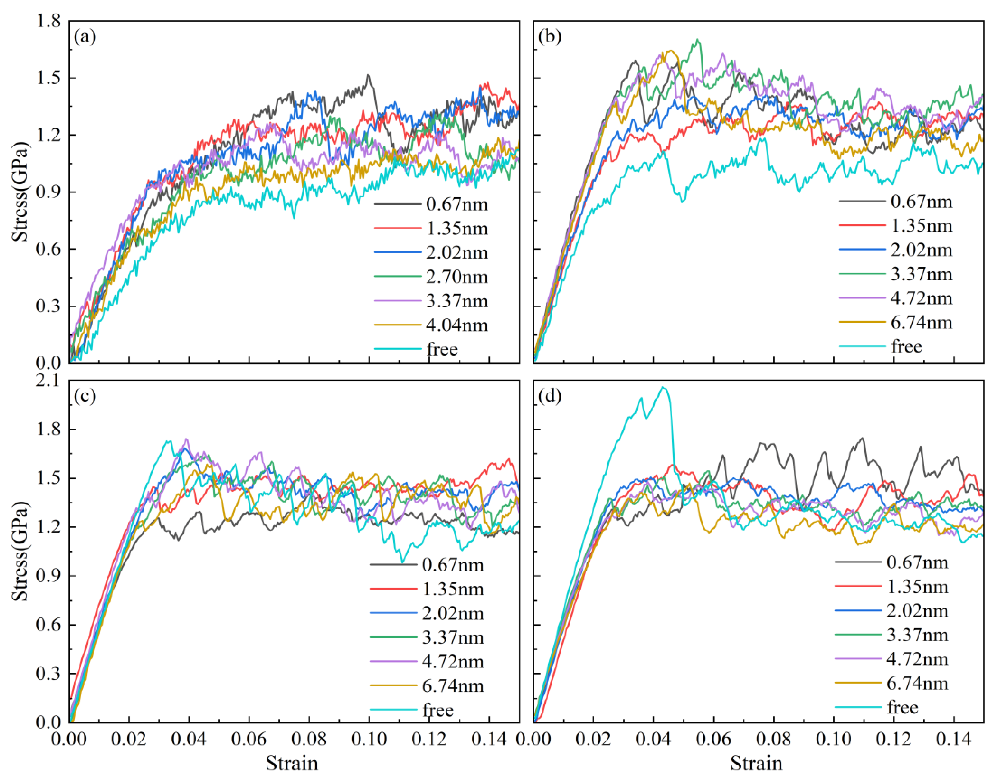
Figure 3.
The average flow stress variation curve of nanotwin AgPd alloy with different twin spacing during compression. (a) d=5.50 nm; (b) d=8.24 nm;(c) d=11.00 nm;(d) d=13.76 nm.
Figure 3.
The average flow stress variation curve of nanotwin AgPd alloy with different twin spacing during compression. (a) d=5.50 nm; (b) d=8.24 nm;(c) d=11.00 nm;(d) d=13.76 nm.
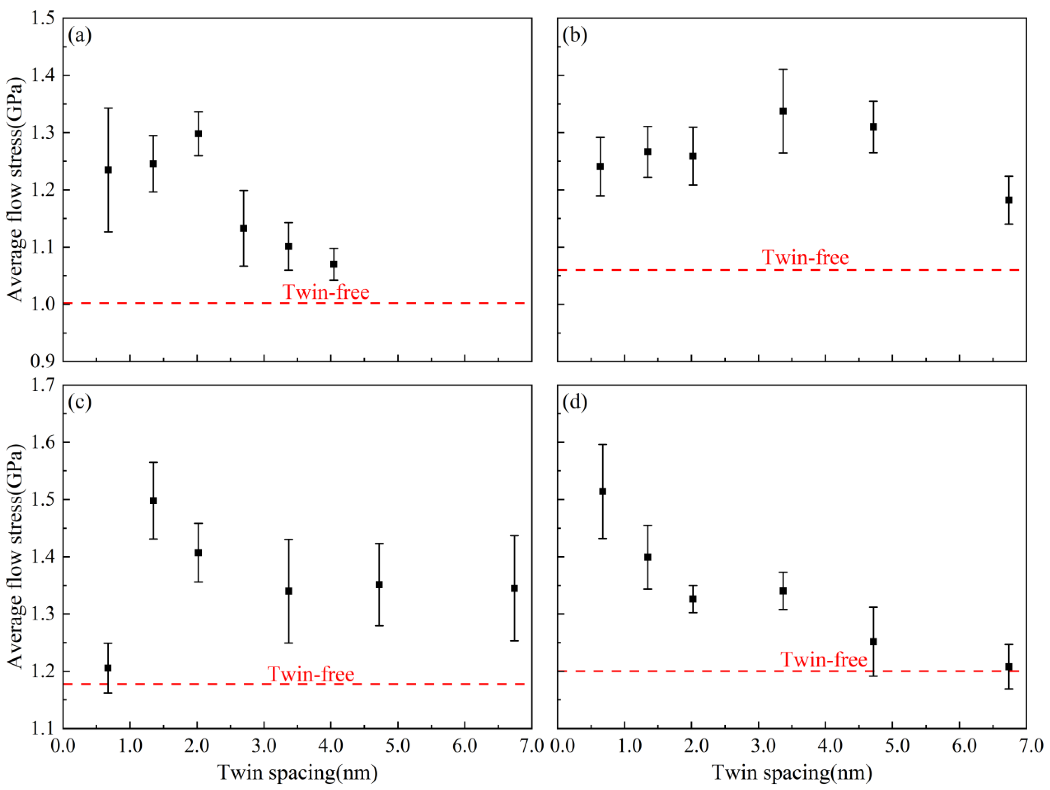
Figure 4.
The statistical chart of atomic proportions in various structures of AgPd alloy with different twin spacing after relaxation.
Figure 4.
The statistical chart of atomic proportions in various structures of AgPd alloy with different twin spacing after relaxation.
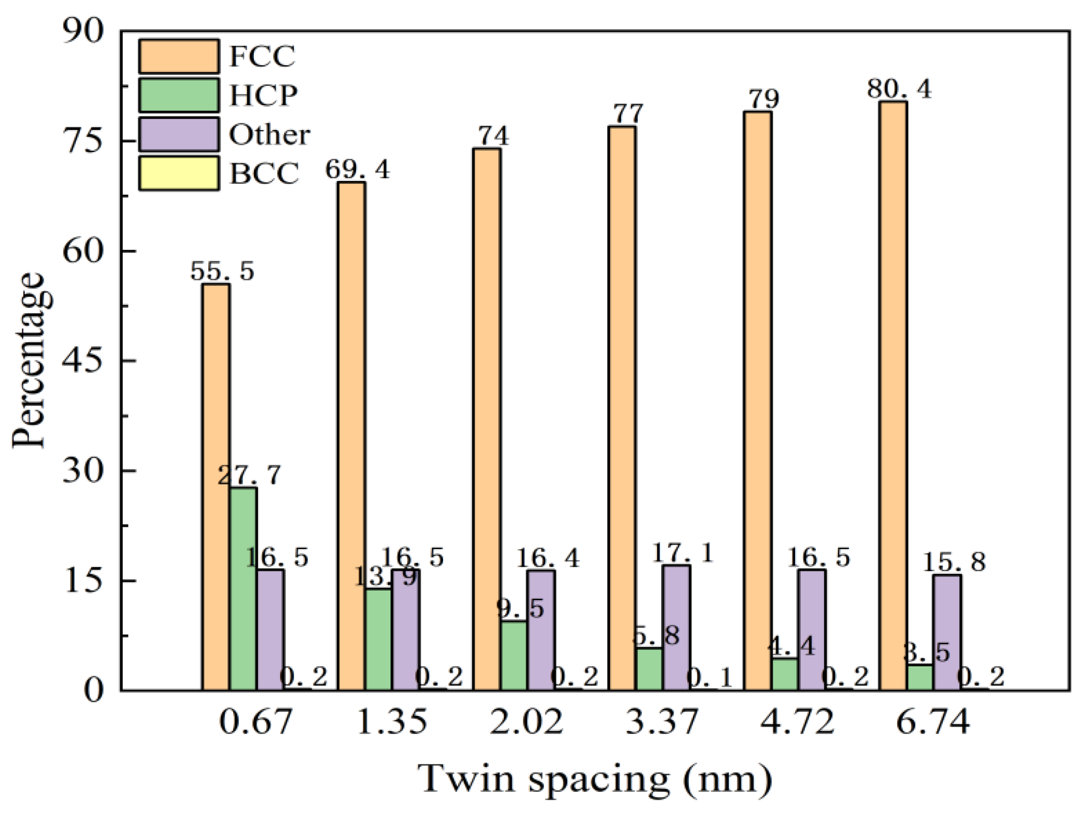
Figure 5.
The variation curve of atomic changes and stress with strain in the structure of nanotwin AgPd alloy with different twin spacing. (a) λ=0.67 nm;(b) λ=1.35 nm;(c) λ=2.02 nm;(d) λ=3.37 nm;(e) λ=4.72 nm;(f) λ=6.74 nm.
Figure 5.
The variation curve of atomic changes and stress with strain in the structure of nanotwin AgPd alloy with different twin spacing. (a) λ=0.67 nm;(b) λ=1.35 nm;(c) λ=2.02 nm;(d) λ=3.37 nm;(e) λ=4.72 nm;(f) λ=6.74 nm.
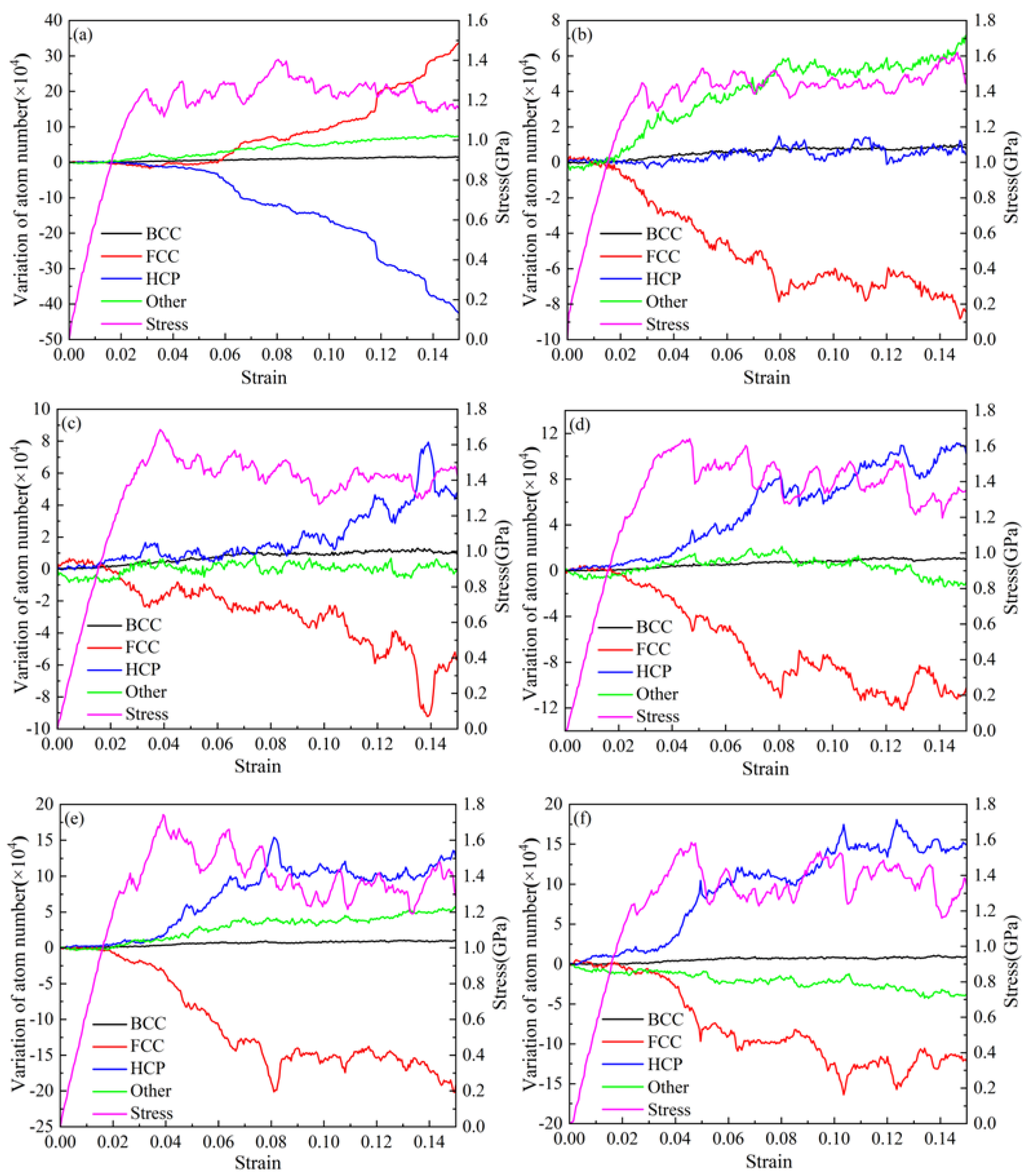
Figure 6.
The variation curve of the length of various types of dislocation lines with strain in nanotwin AgPd alloy. (a) λ=0.67 nm;(b) λ=1.35 nm;(c) λ=2.02 nm;(d) λ=3.37 nm;(e) λ=4.72 nm;(f) λ=6.74 nm.
Figure 6.
The variation curve of the length of various types of dislocation lines with strain in nanotwin AgPd alloy. (a) λ=0.67 nm;(b) λ=1.35 nm;(c) λ=2.02 nm;(d) λ=3.37 nm;(e) λ=4.72 nm;(f) λ=6.74 nm.
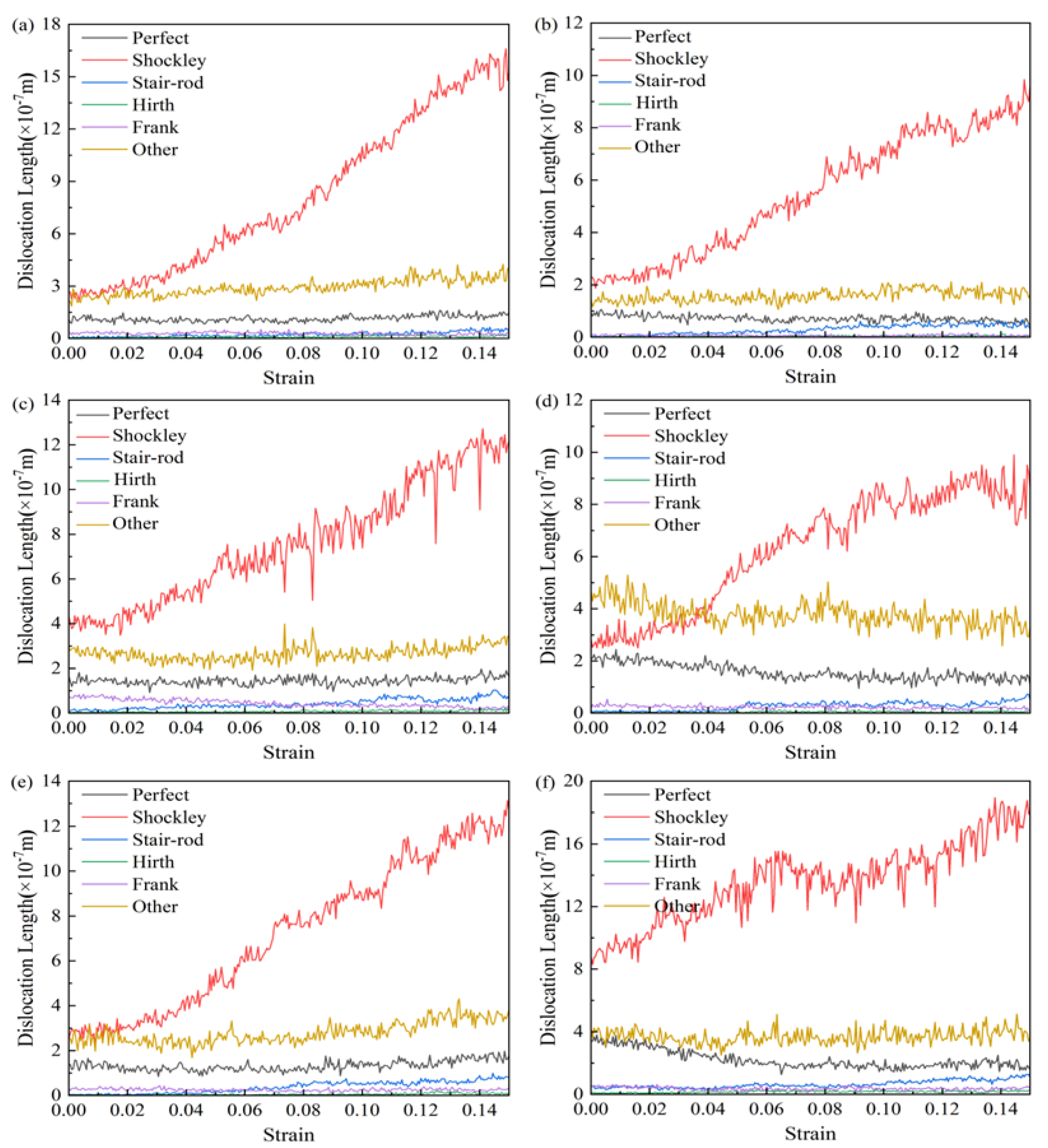
Figure 7.
The variation curve of dislocation density with strain in nanotwin AgPd alloys with different twin spacing.
Figure 7.
The variation curve of dislocation density with strain in nanotwin AgPd alloys with different twin spacing.
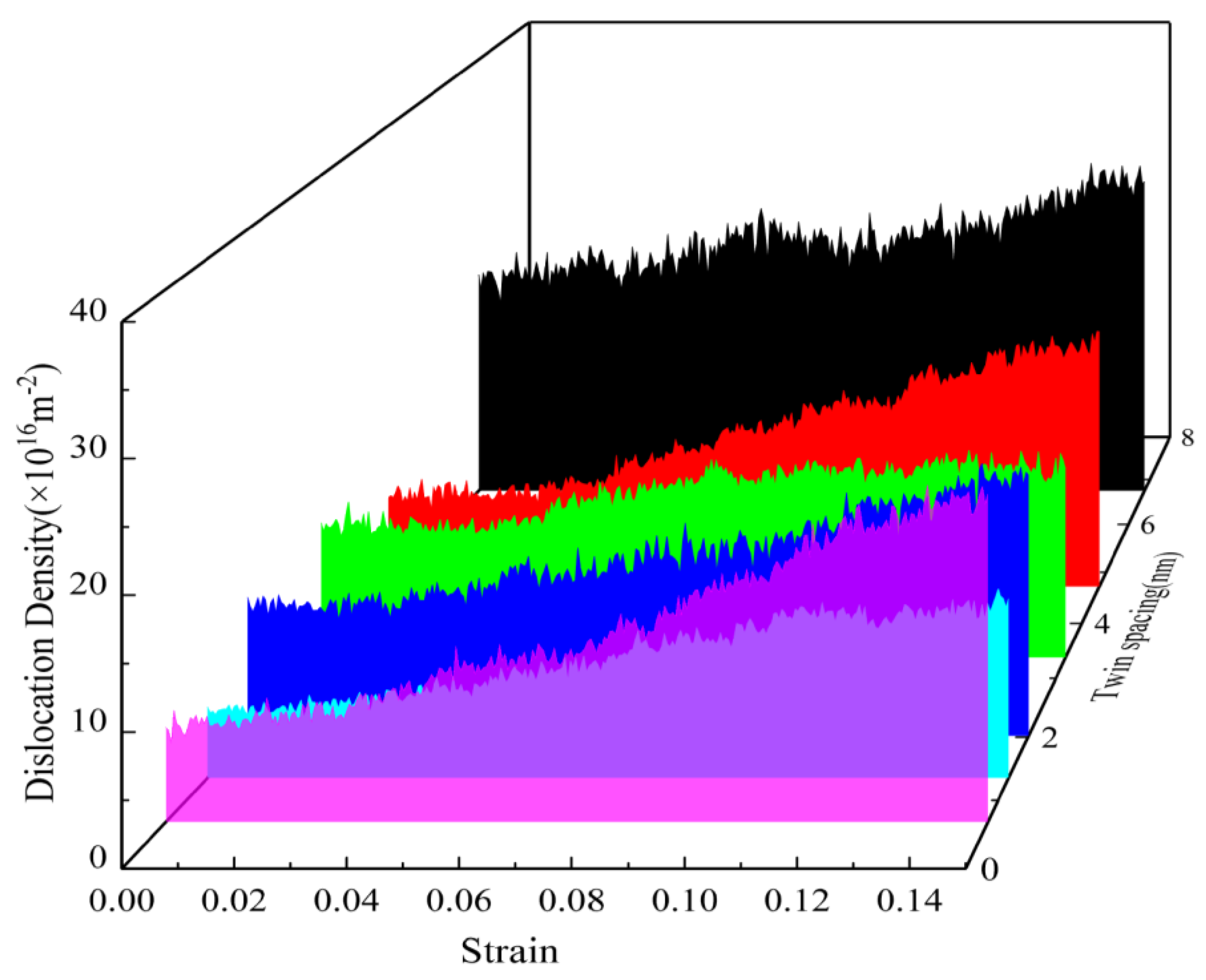
Figure 8.
The nanocrystalline polycrystalline AgPd alloy with average grain size of 11.00 nm exhibits compressed atomic diagrams at 0% (a), 3.00% (b), 12.00% (c), and 15.00% (d), respectively. a1-d1 and a2-d2 are corresponding shear strain and displacement vector diagrams, respectively.
Figure 8.
The nanocrystalline polycrystalline AgPd alloy with average grain size of 11.00 nm exhibits compressed atomic diagrams at 0% (a), 3.00% (b), 12.00% (c), and 15.00% (d), respectively. a1-d1 and a2-d2 are corresponding shear strain and displacement vector diagrams, respectively.
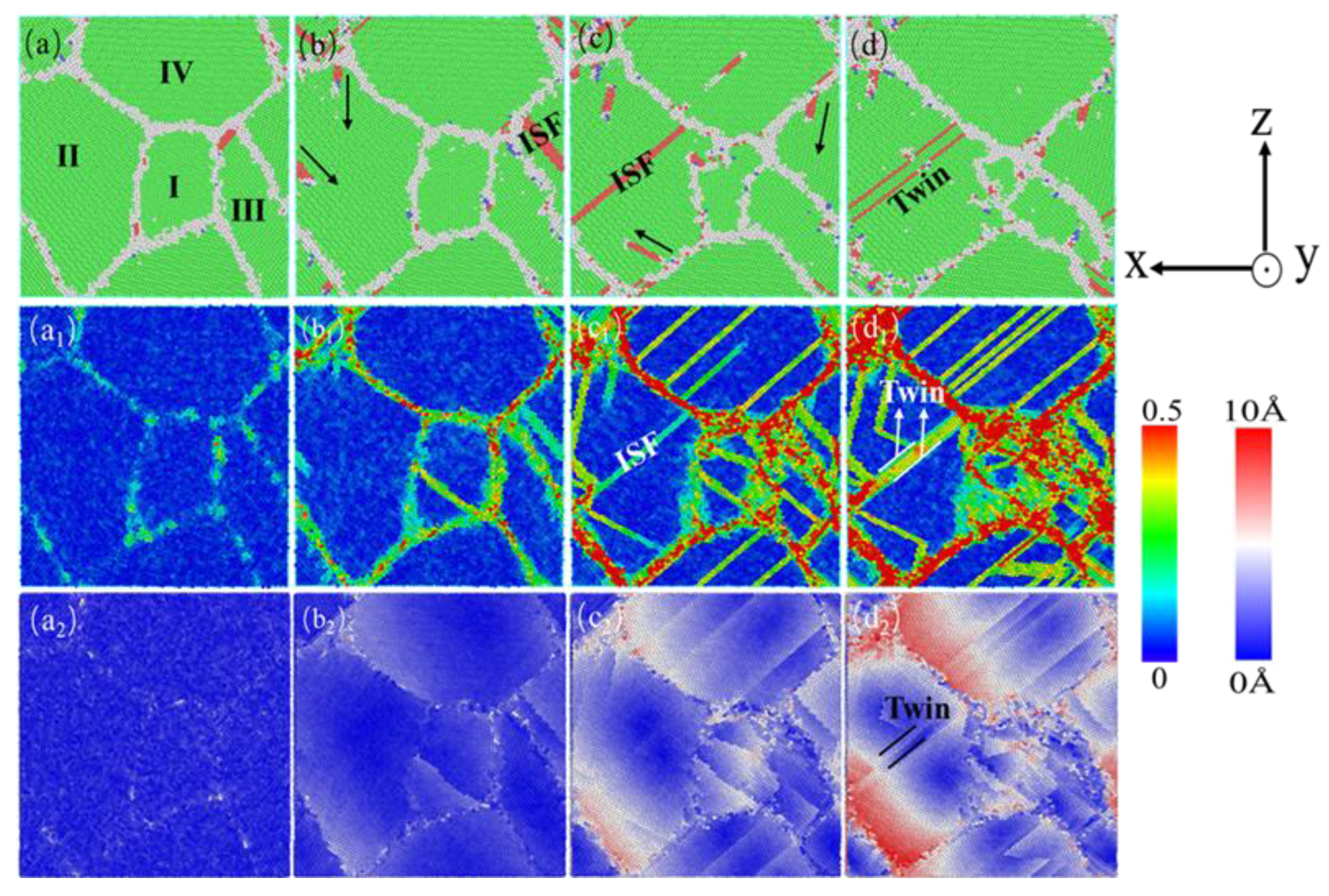
Figure 9.
The nanocrystalline polycrystalline AgPd alloy with a twin spacing of 0.67 nm and an average grain size of 11.00 nm exhibits compressed atomic diagrams at 0% (a), 3.00% (b), 12.00% (c), and 15.00% (d), respectively. a1-d1 and a2-d2 are corresponding shear strain and displacement vector diagrams, respectively.
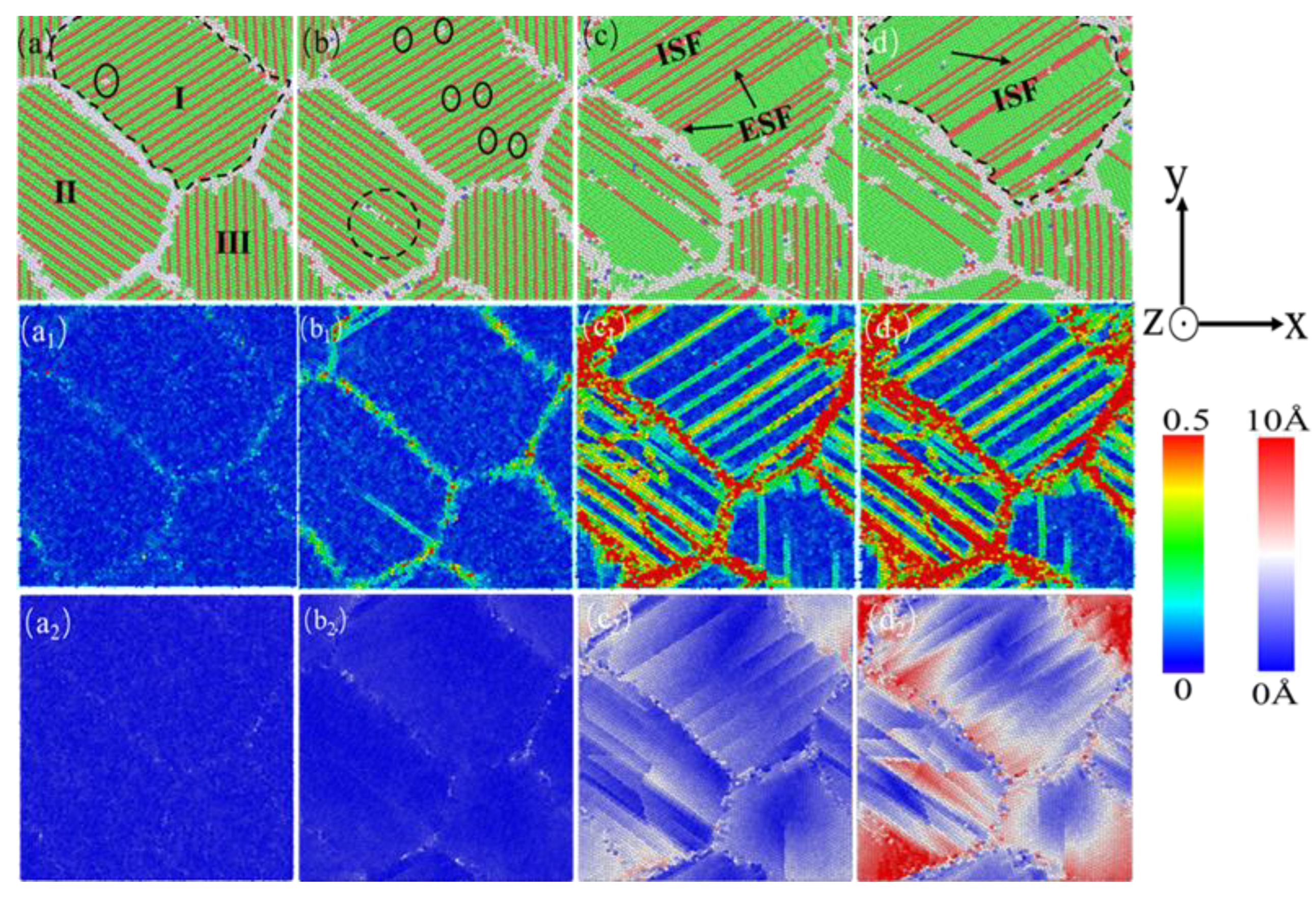
Figure 10.
The nanocrystalline polycrystalline AgPd alloy with a twin spacing of 1.34 nm and an average grain size of 11.00 nm exhibits compressed atomic diagrams at 0% (a), 2.85% (b), 8.30% (c), and 15.00% (d), respectively. a1-d1 and a2-d2 are corresponding shear strain and displacement vector diagrams, respectively.
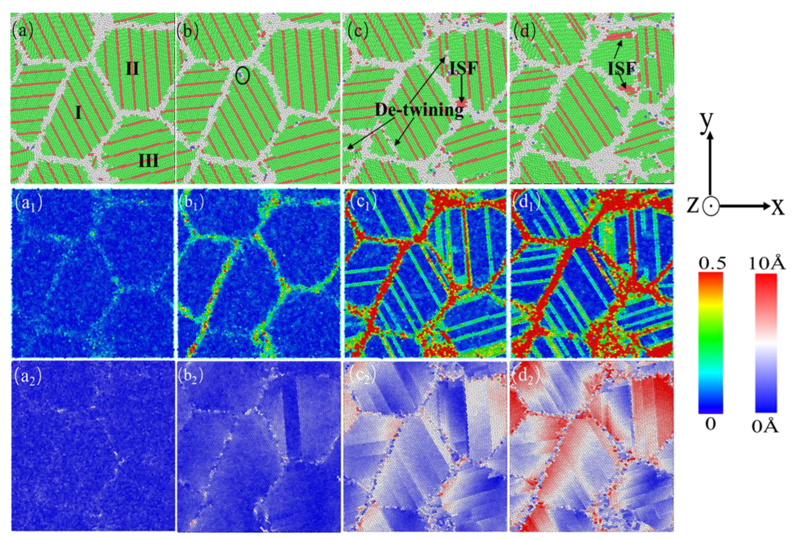
Figure 11.
The nanocrystalline polycrystalline AgPd alloy with a twin spacing of 6.74 nm and an average grain size of 11.00 nm exhibits compressed atomic diagrams at 0% (a), 2.45% (b), 8.55% (c), and 15.00% (d), respectively. a1-d1 and a2-d2 are corresponding shear strain and displacement vector diagrams, respectively.
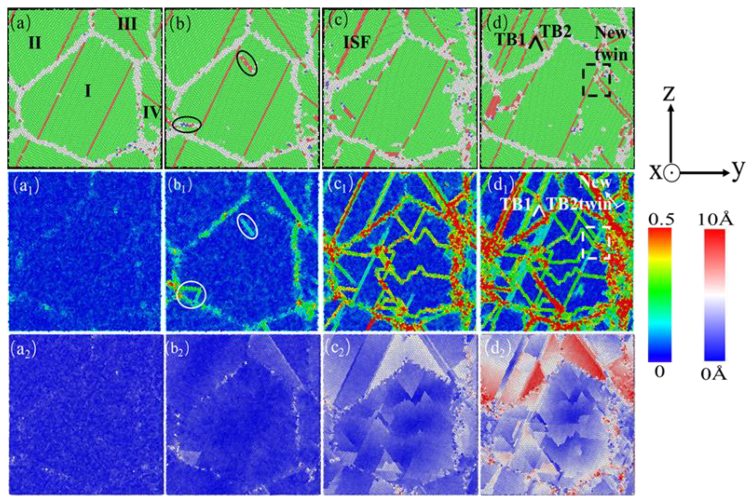
Figure 12.
The stress-strain curves of nanotwin AgPd alloy under compression at different temperatures, (a)10 K;(b)100 K;(c)300 K;(d)500 K.
Figure 12.
The stress-strain curves of nanotwin AgPd alloy under compression at different temperatures, (a)10 K;(b)100 K;(c)300 K;(d)500 K.
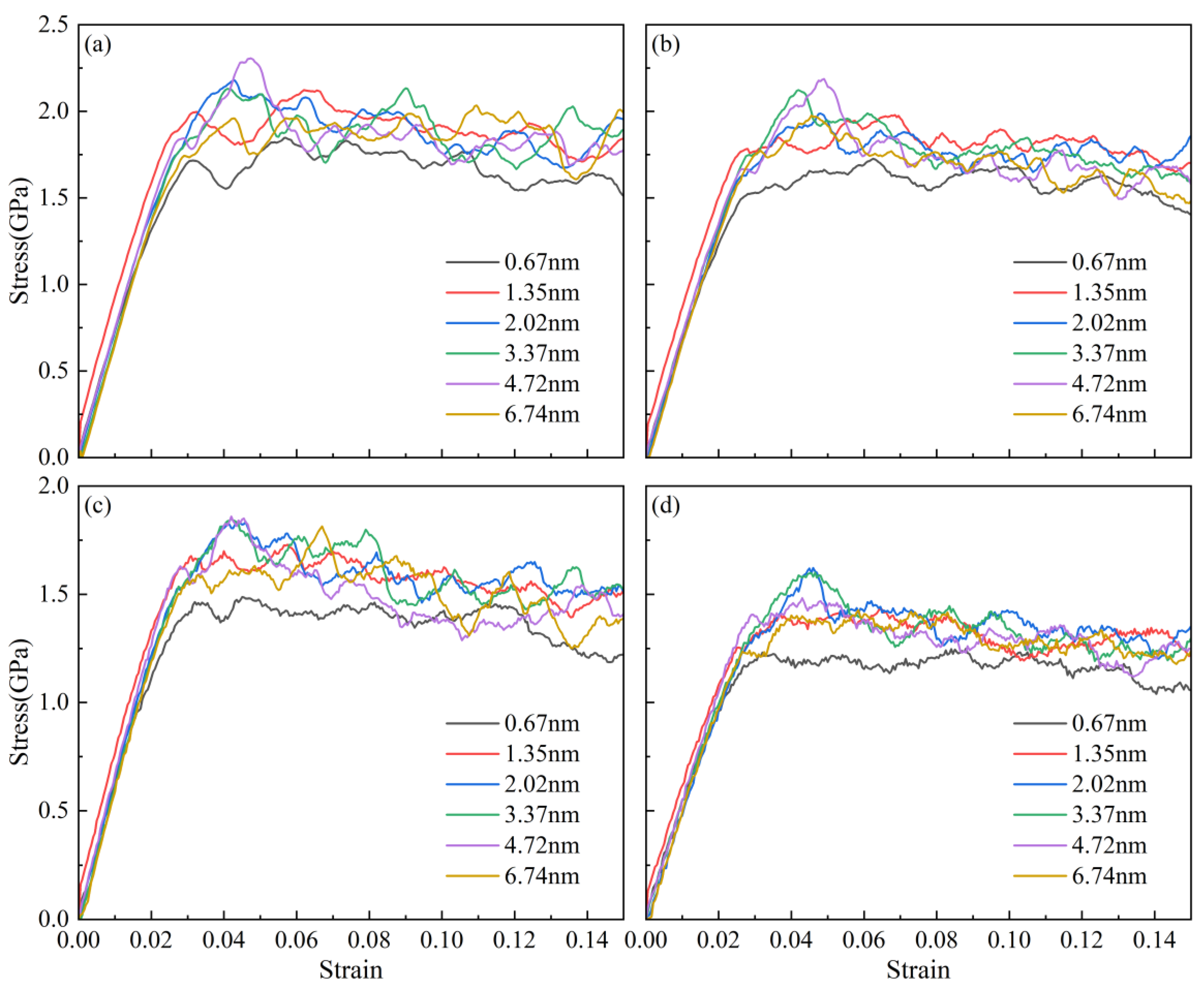
Figure 13.
The curve of the change in Young's modulus (a) and average flow stress (b) of nanotwin AgPd alloy at different temperatures with the variation of nanotwin spacing.
Figure 13.
The curve of the change in Young's modulus (a) and average flow stress (b) of nanotwin AgPd alloy at different temperatures with the variation of nanotwin spacing.
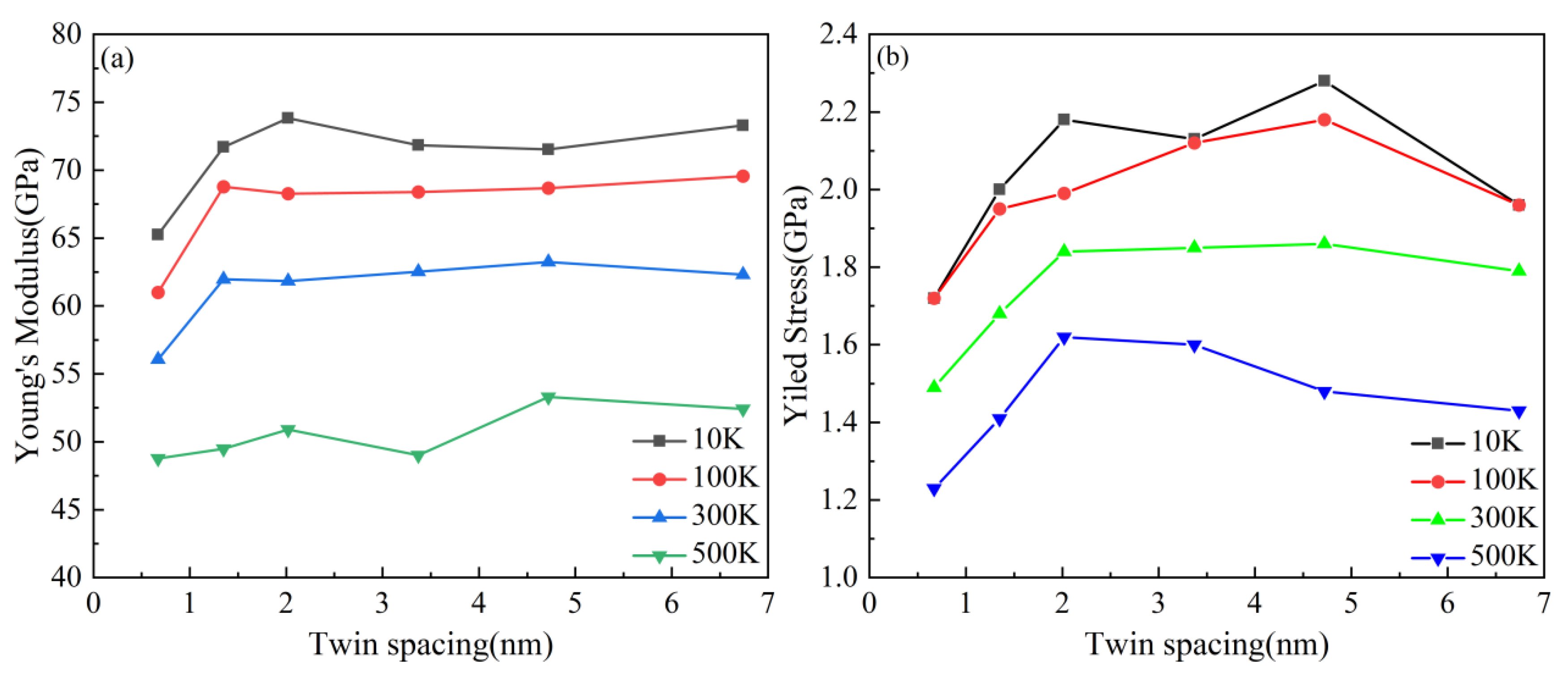
Figure 14.
Statistical charts of the atomic proportions of each structure in nanotwin AgPd alloy after relaxation at different temperatures.
Figure 14.
Statistical charts of the atomic proportions of each structure in nanotwin AgPd alloy after relaxation at different temperatures.
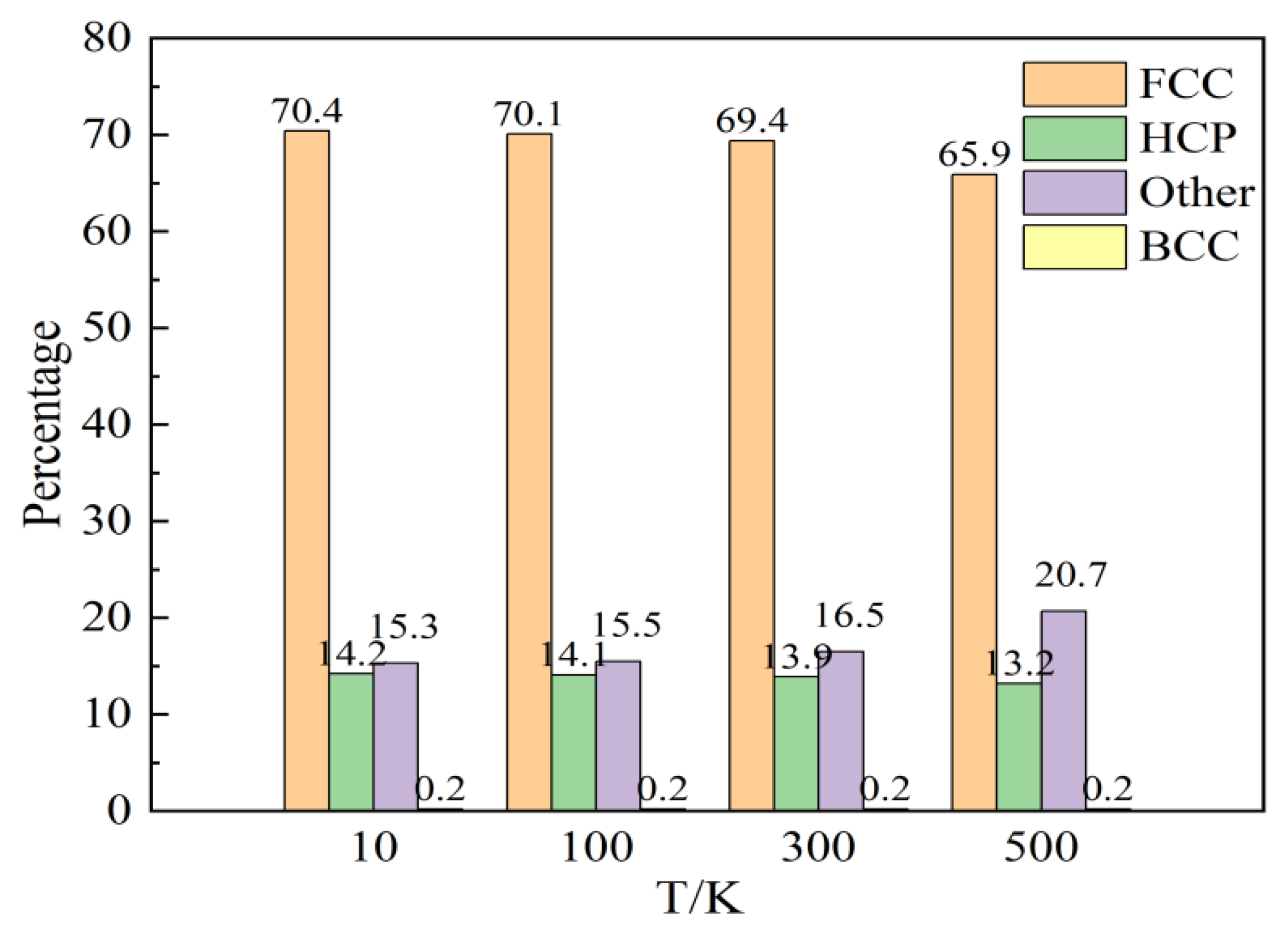
Figure 15.
The variation curves of atomic changes and stress with strain in the structure of nanotwin AgPd alloy at different temperatures. (a)10 K;(b)100 K;(c)300 K;(d)500 K.
Figure 15.
The variation curves of atomic changes and stress with strain in the structure of nanotwin AgPd alloy at different temperatures. (a)10 K;(b)100 K;(c)300 K;(d)500 K.
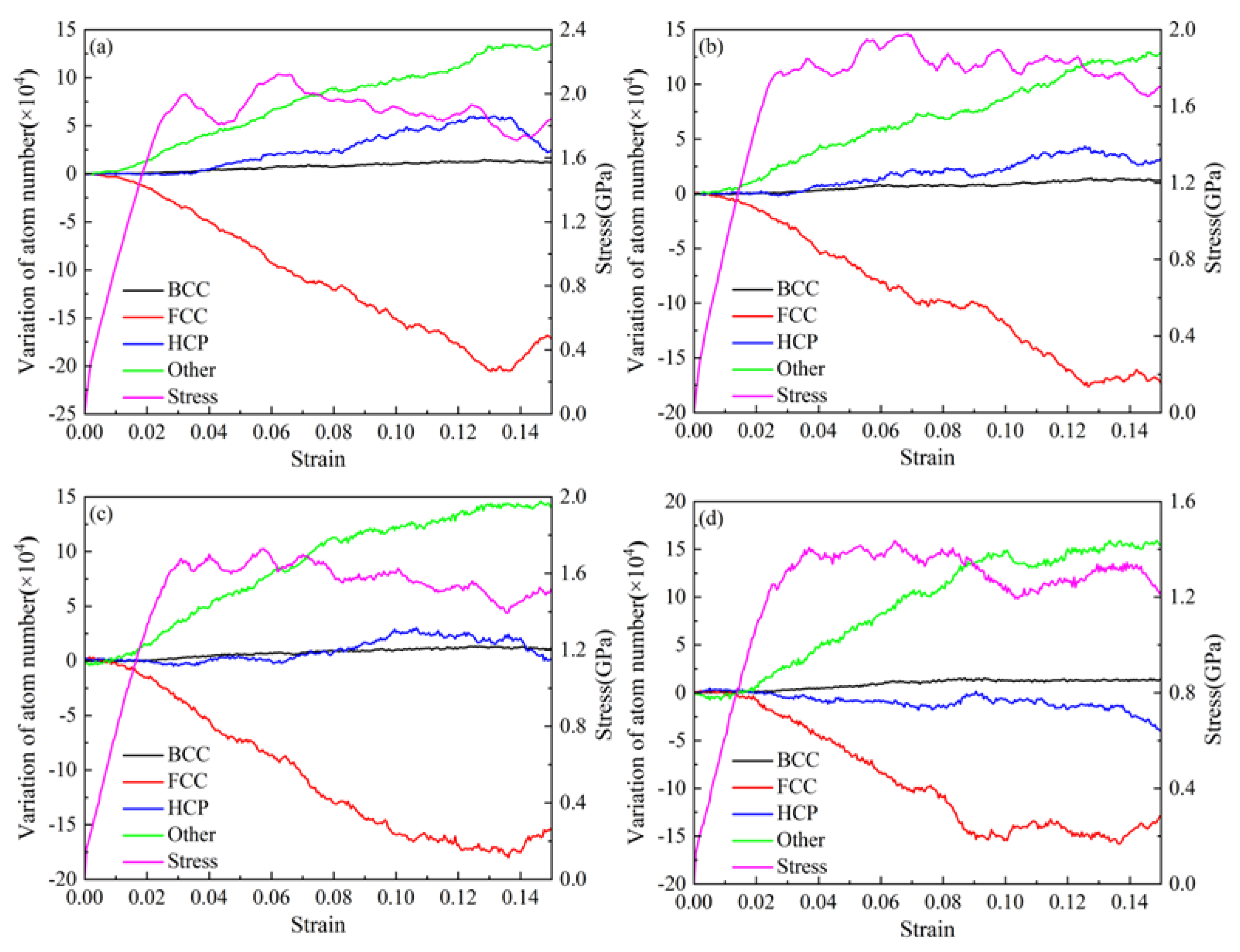
Figure 16.
The variation curve of the length of various types of dislocation lines with strain in nanotwin AgPd alloy at different temperatures. (a)10 K;(b)100 K;(c)300 K;(d)500 K.
Figure 16.
The variation curve of the length of various types of dislocation lines with strain in nanotwin AgPd alloy at different temperatures. (a)10 K;(b)100 K;(c)300 K;(d)500 K.
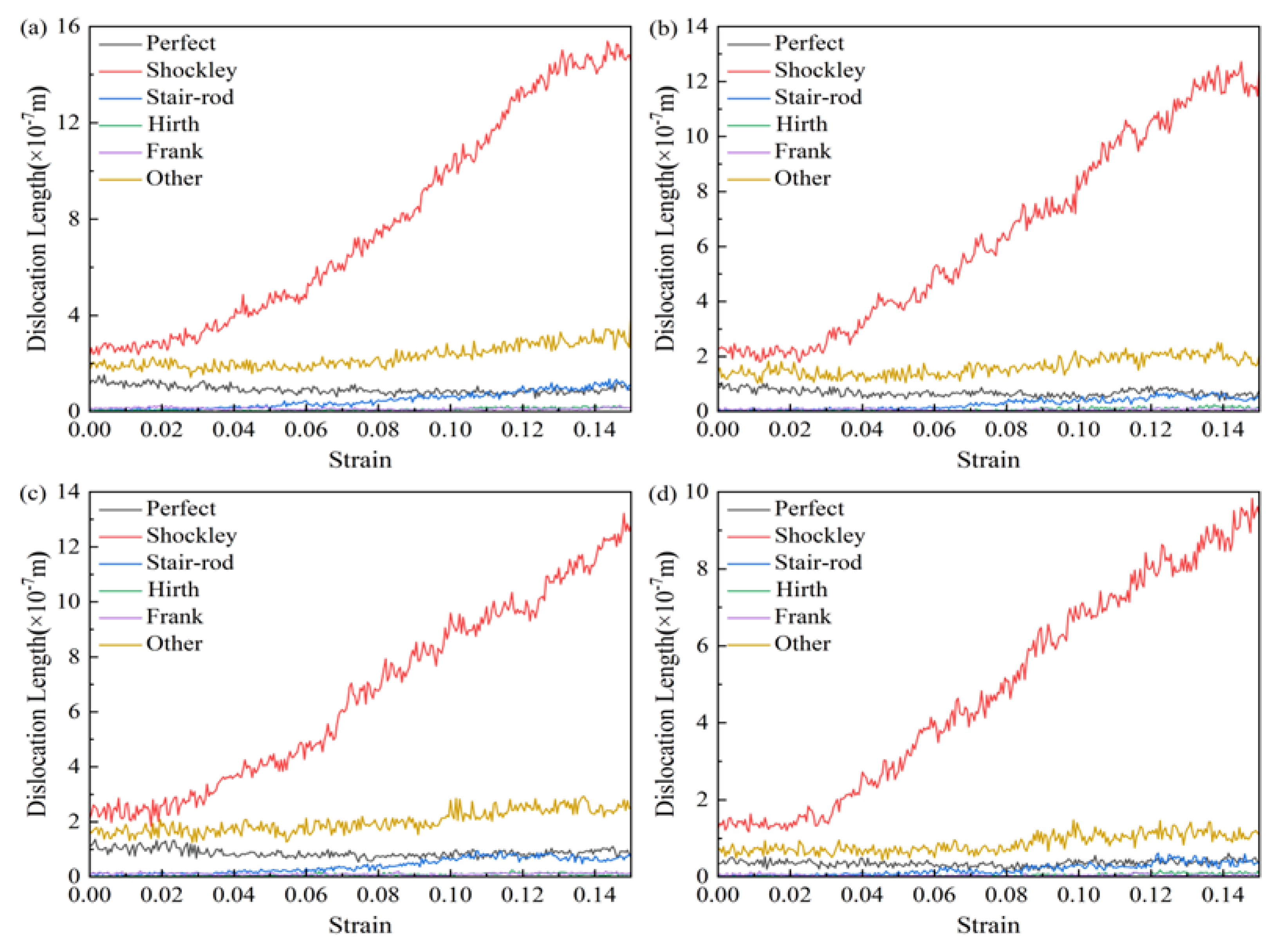
Figure 17.
The variation curve of dislocation density with strain in nanotwin AgPd alloy at different temperatures.
Figure 17.
The variation curve of dislocation density with strain in nanotwin AgPd alloy at different temperatures.
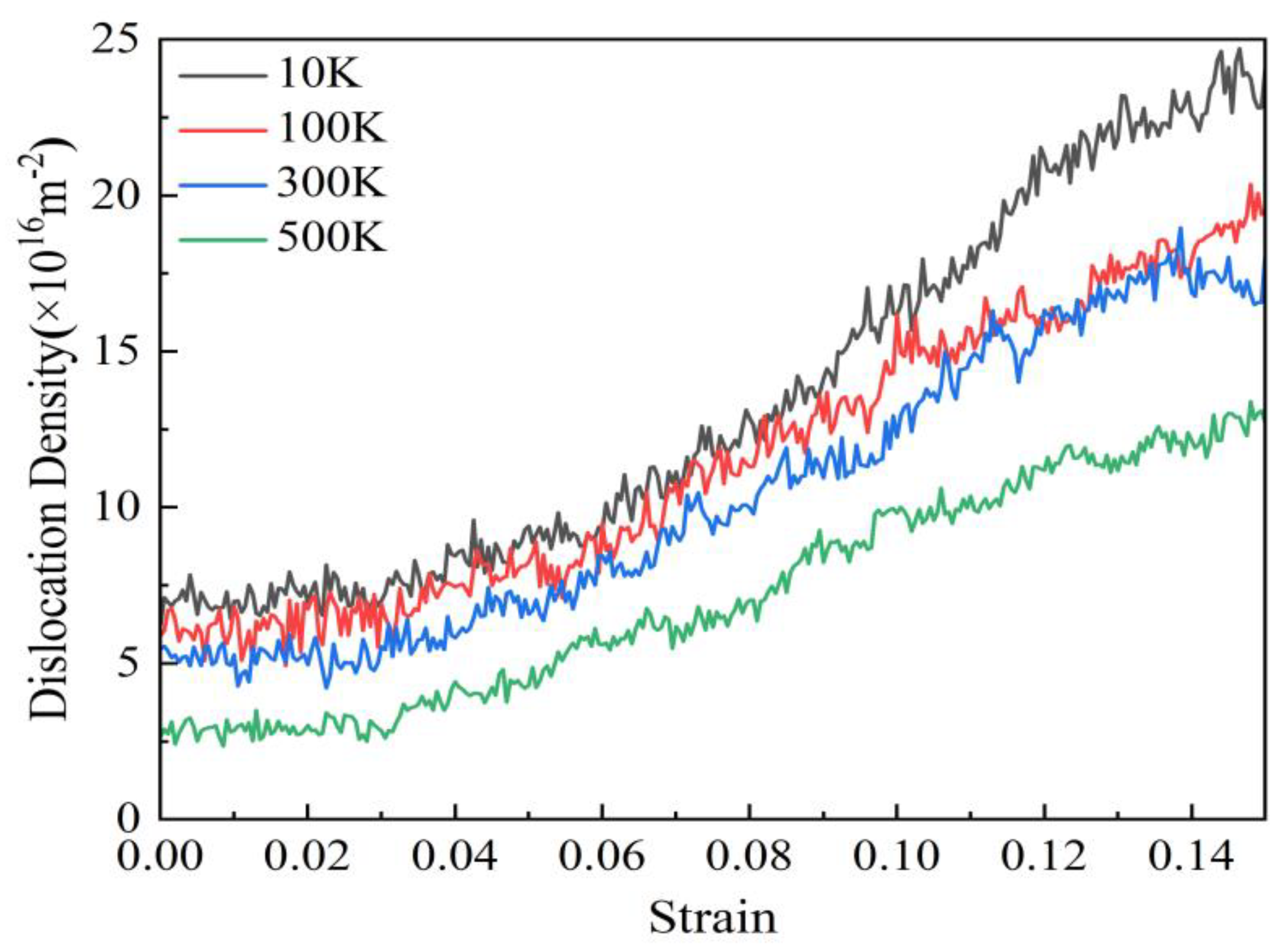
Figure 18.
The compressed atomic diagrams of nanotwin AgPd alloy at different temperatures at strains of 0% (a, a1, a2), 2.60% (b, b1, b2), 10.00% (c, c1, c2), and 15.00% (d, d1, d2).
Figure 18.
The compressed atomic diagrams of nanotwin AgPd alloy at different temperatures at strains of 0% (a, a1, a2), 2.60% (b, b1, b2), 10.00% (c, c1, c2), and 15.00% (d, d1, d2).
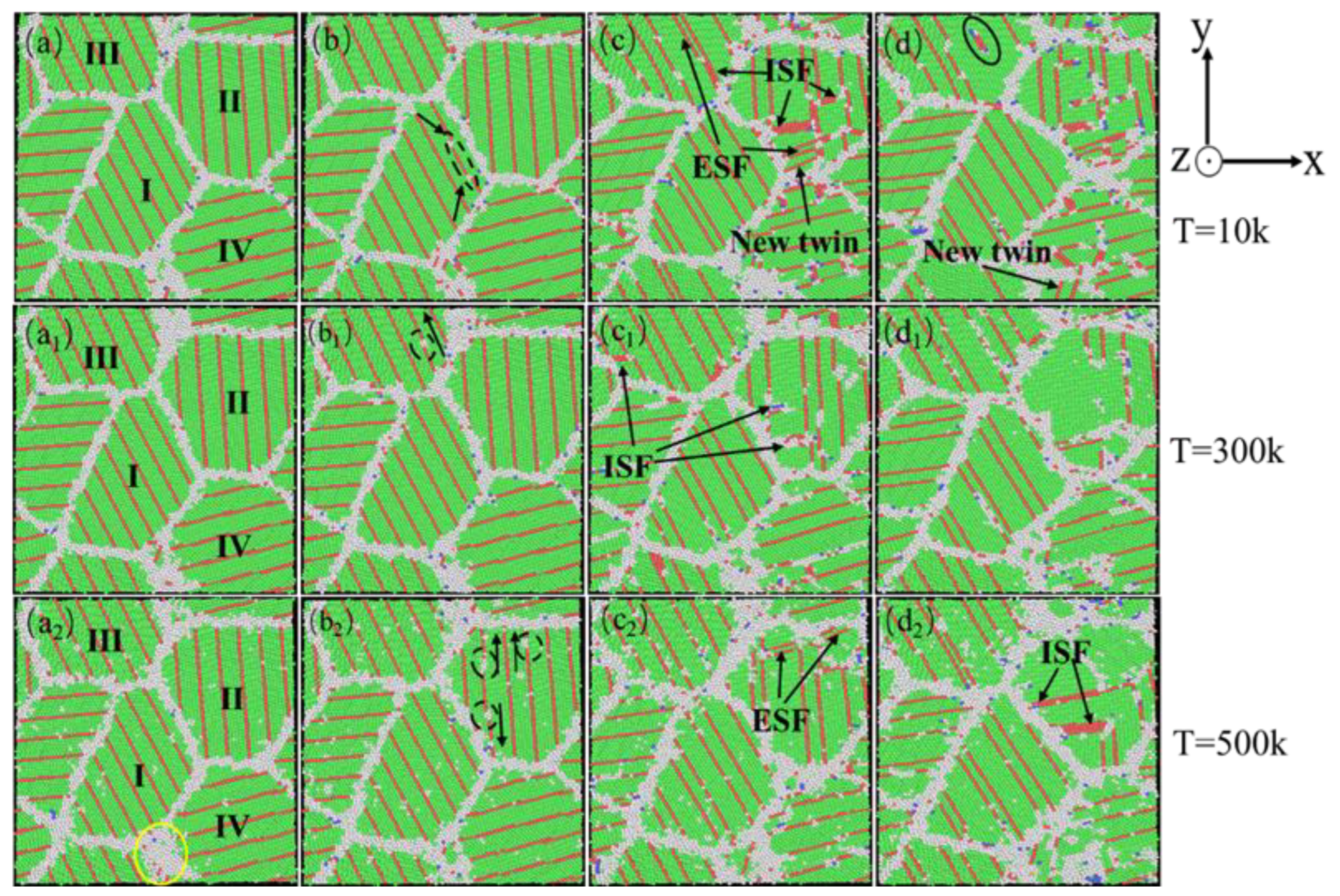
Figure 19.
The compressed atomic diagrams of a nanocrystalline polycrystalline AgPd alloy with a twin spacing of 0.67 nm and an average grain size of 11.00 nm at 0% (a), 3.15% (b), 13.05% (c), and 15.00% (d) strain are presented. a1-d1 and a2-d2 are the corresponding shear strain diagrams and displacement vector diagrams, respectively.
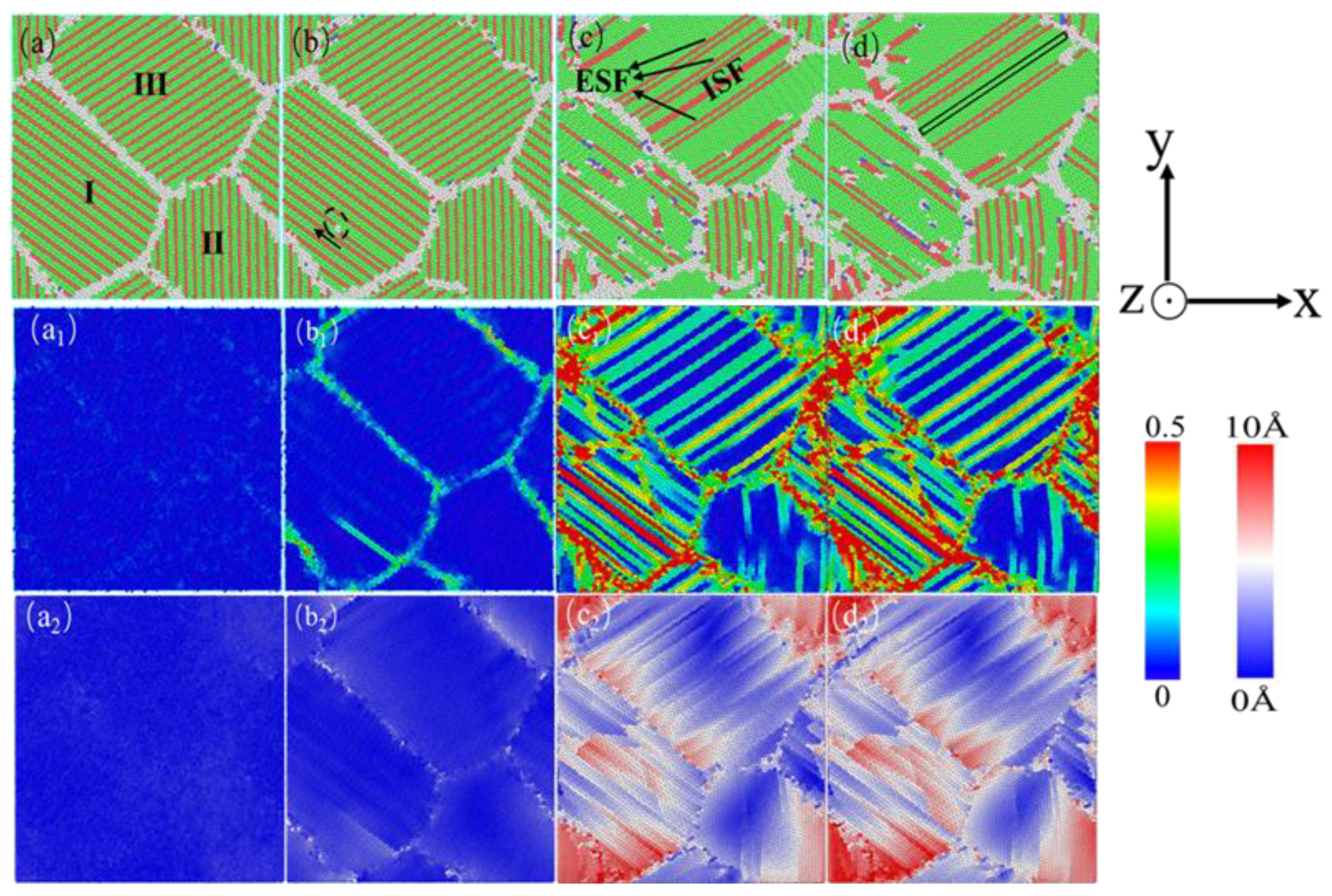
Figure 20.
The compressed atomic diagrams of a nanocrystalline polycrystalline AgPd alloy with a twin spacing of 0.67 nm and an average grain size of 11.00 nm at 0% (a), 3.15% (b), 13.05% (c), and 15.00% (d) strain are presented. a1-d1 and a2-d2 are the corresponding shear strain diagrams and displacement vector diagrams, respectively.
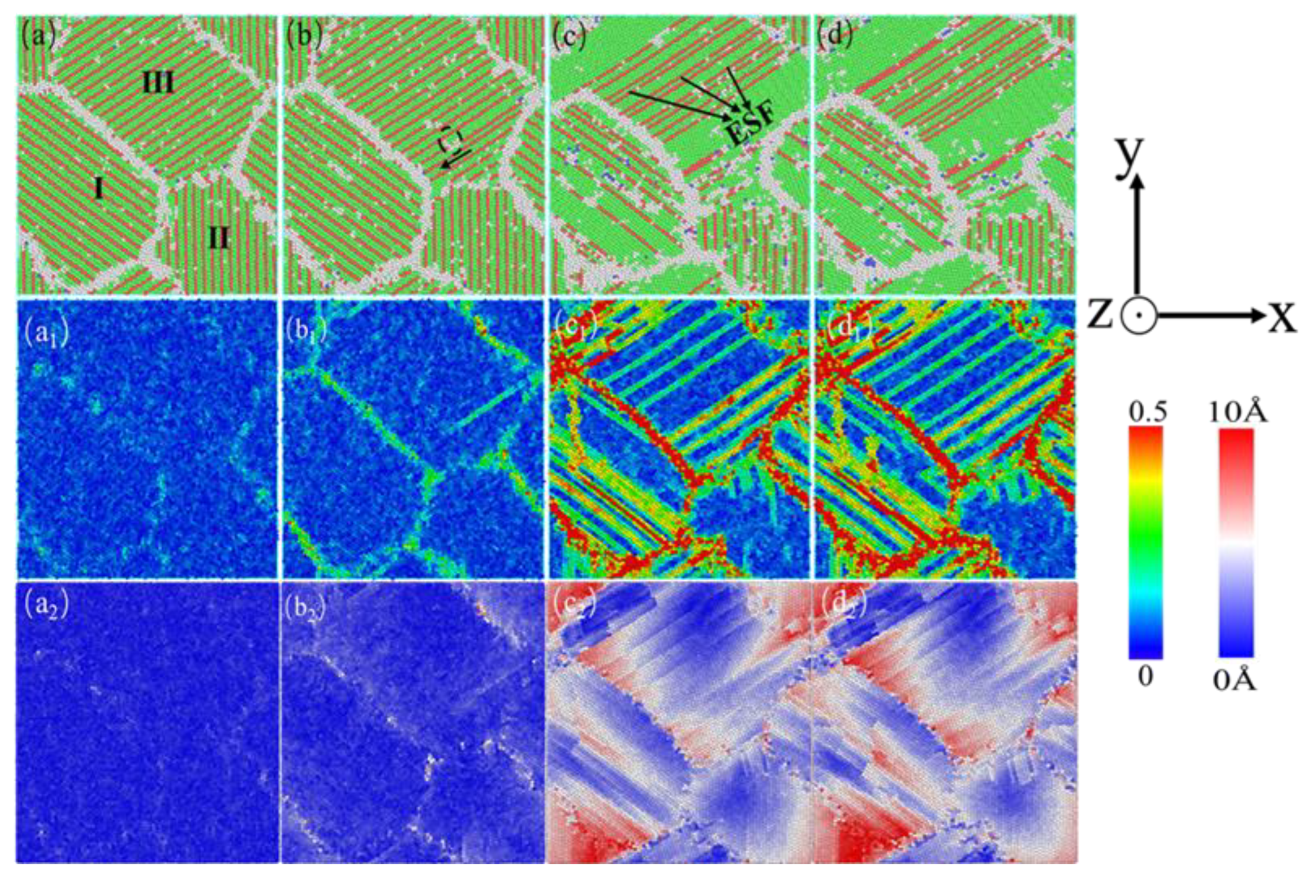
Table 1.
Initial configuration related parameters of nanotwin AgPd alloy.
| Alloy | Average grain size (d/nm) | Number of atoms | Twin spacing (λ/nm) | |||||
| AgPd | 5.00 | 67900 | 0.67 | 1.35 | 2.02 | 2.70 | 3.37 | 4.04 |
| 8.24 | 228500 | 0.67 | 1.35 | 2.02 | 3.37 | 4.72 | 6.74 | |
| 11.00 | 542500 | 0.67 | 1.35 | 2.02 | 3.37 | 4.72 | 6.74 | |
| 13.76 | 1061000 | 0.67 | 1.35 | 2.02 | 3.37 | 4.72 | 6.74 | |
Disclaimer/Publisher’s Note: The statements, opinions and data contained in all publications are solely those of the individual author(s) and contributor(s) and not of MDPI and/or the editor(s). MDPI and/or the editor(s) disclaim responsibility for any injury to people or property resulting from any ideas, methods, instructions or products referred to in the content. |
© 2024 by the authors. Licensee MDPI, Basel, Switzerland. This article is an open access article distributed under the terms and conditions of the Creative Commons Attribution (CC BY) license (http://creativecommons.org/licenses/by/4.0/).
Copyright: This open access article is published under a Creative Commons CC BY 4.0 license, which permit the free download, distribution, and reuse, provided that the author and preprint are cited in any reuse.


