
Submitted:
11 October 2024
Posted:
11 October 2024
You are already at the latest version
Abstract
Novel double-impurity doping process for silicon (Si) surfaces was developed, utilizing nanosecond-laser melting of a top 11-nm thick gold (Au) film and a Si wafer substrate in a laser plasma-activated liquid-nitrogen (LN) environment. Scanning electron microscopy revealed the fluence- and exposure-independent surface micro-spike topography, while energy-dispersive x-ray spectroscopy identified minor Au (0.05 at. %) and major N (1-2 at. %) dopants, localized within a 0.5-m thick surface layer, and slight surface post-oxidation of the micro-relief (oxygen (O), 1.5-2.5 at. %). X-ray photoelectron spectroscopy identified bound surface (SiNx) and bulk doping chemical states of the introduced nitrogen (10 at. %), metallic (<0.01 at. %) and cluster (<0.1 at. %) forms of gold dopant, and evaluated their depth distributions, strongly affected by the competition between gold dopant in its marginal local concentrations and other more abundant dopants (N, O). 532-nm Raman micro-spectroscopy indicated the slight reduction of the crystalline order revealed in the second-order Si phonon band, nanoscale dimensions of the resolidified Si nano-crystallites envisioned by the main Si optical-phonon peak, negligible a-Si abundance and a low-wavenumber peak of Si3N4 structure. In contrast, Fourier-transform infrared (FT-IR) 2D-mapping exhibited the only broad structureless absorption bands in the range of 600-5500 cm-1 related to dopant absorption and light-trapping in the surface micro-relief. The room-temperature electrical characteristics of the laser-double-doped Si layer – carrier mobility of 1050 cm2/Vs and background carrier sheet concentration 21010 cm-2 (bulk concentration 1014-1015 cm-3) – are superior regarding previously reported parameters of nitrogen-implanted/annealed Si samples. This novel facile double-element laser-doping procedure paves the way toward local mask-less on-demand introduction of multiple intra-gap intermediate donor and acceptor bands in Si, providing its related multi-wavelength IR photoconductivity for optoelectronic applications.
Keywords:
nanosecond laser
; Si wafer
; top Au film
; liquid-nitrogen environment
; Au/N double-element doping
; nano-recrystallization of Si
; mid-IR-vis absorption
1. Introduction
Nowadays silicon (Si) is reviving as a basic nano- and optoelectronic material, being a key component material in CMOS-compatible planar photonic integrated circuits [1], extended in their functionality by heterogeneous integration with III-V heterostructures [2]. Photonic integrated circuits are demanded in ultrafast telecommunication and other signal-processing modules, utilizing ultimate speed of light, ultrafast switching etc. [3].
Hyperdoping of semiconductors, including Si, through non-equilibrium condensed – solid- or liquid- − phase mechanisms, such as ion implantation [4,5], pulsed laser melting of surface dopant layers along with the semiconductor substrate [6,7] or doping in pulsed laser-activated chemically-active fluids [8,9,10], was broadly utilized to enhance p-n-junction functionality (dimensions, response time, etc.) [11] or specific near-IR or mid-IR light absorption for their optoelectronic response [12,13]. In the latter case, the dopant could form a rather deep intermediate donor (acceptor) impurity band in the semiconductor bandgap [14], still merging with the corresponding conduction (valence) band at high impurity concentrations ~1020-1021 cm-3 [15], resulting in an “insulator-to-conductor” transition [16]. Additionally, the related spontaneous amorphization of the material due to internal impurity-induced stresses [17], considerable reduction of carrier mobility due their scattering on impurity centers or thermally-ionized free carriers [18], and their trapping at the deep impurity-related traps [19] set a natural doping limit at high doping concentrations, requiring elaborate management of impurity intragap energetic states via control of dopant concentrations, chemical and charge states [20,21]. Double or even multiple doping of semiconductors opens a way to overcome the concentration-related “insulator-to-conductor” transition obstacle by formation of a few intermediate donor (acceptor) bands across the semiconductor bandgap [22]. So far, double doping was performed, minimum, in two steps – one for each dopant [23], with the interference (synergy or competition) of the different dopants during the doping process being still a “black-box” issue, potentially depending on chemical, concentration and other factors.
Recently, Si wafer was laser-doped by nitrogen (N) in a laser plasma-activated liquid-nitrogen (LN) environment [24], similarly to boron carbide in previous studies [10]. Nitrogen impurity is known as a key dopant for improving Si crystalline structure by enhancing oxygen precipitation to improve the intrinsic gettering ability of silicon wafers [25], locking dislocations to increase mechanical strength [26] and annihilating microdefects [27] (voids and interstitial-type dislocation aggregates via accumulation of vacancies in N-V complexes [28]), both in floating-zone-grown and Czochralski-grown silicon crystals. Bulk doping with nitrogen atoms in substitutional (Ns) positions as deep donor centers could occur (not only in dislocations, grain boundaries and cellular structure), when the critical content of nitrogen ( ~1015 atom/cm3 [29]) is locally exceeded in the Si crystal [30]. By itself, N-doped Si exhibits strong sub-bandgap infrared (IR) absorption [31,32], suitable for empowering optoelectronic, photovoltaic and detector performance [33,34] and offering a wide range of potential applications.
However, the challenging introduction of N into Si via non-equilibrium ion implantation meets difficulties in producing high N concentrations due to the very low solid and liquid solubility limits of only 4.5×10¹⁵ and 6.0×10¹⁸ atoms/cm3 [35], respectively, crystal damage and amorphization [36], activation of interstitial N into substitutional sites [37], with the dominant and most stable N defect in Si being the di-interstitial pair (Ni-Ni) [38]. Then, additional laser annealing converts nitrogen into active Nsform, with the highest achieved total N concentration in Si to date, of 0.5 ± 0.2 at. % (2.5×10²⁰ at./cm3) [39]. For the maximal implanted nitrogen concentrations of below 1020 atoms/cm-3 Si remains crystalline, but amorphous Si and SiN appear for nitrogen concentrations above 3×10²⁰ atoms/cm-3, transforming into precipitated Si3N4 upon annealing at 10000C or in continuous layer of crystalline Si3N4 for concentrations above 4×10²² atoms/cm3 [40,41], while the excess nitrogen could be trapped and make blistering during high-temperature annealing. Alternatively, reactive laser or plasma-enhanced chemical vapor deposition (PECVD) in nitrogen atmosphere, requiring high-energy plasma species to activate nitrogen and subsequent thermal annealing of as-deposited films to improve their crystalline quality, was reported to result in a-Si3N4 films [42,43], promising for fabrication of low-loss waveguides and integrated-photonics elements [44]. Direct laser treatment in low-pressure ammonia [42], high-pressure ammonia or nitrogen gases [45] provided chemical (a-Si3N4 [42]) or doping (up to 6 at. % [45], comparing to 12 at. % by PECVD [31]) nitrifying of Si surface, respectively.
In this study, double doping of Si wafers by nanosecond-laser plasma-mediated nitrifying and nitrogen doping of an Au-film coated, un-doped crystalline Si wafer immersed into liquid nitrogen was explored in different laser treatment regimes and characterized by means of scanning electron microscopy, energy-dispersive x-ray spectroscopy, x-ray photoelectron spectroscopy, IR and Raman/photoluminescence spectroscopy.
2. Materials and Methods
200-μm thick, double-side polished (100) undoped silicon wafer (resistivity >1 kΩ cm) was covered in argon atmosphere by a 11-nm gold (Au) film though magnetron sputtering (SC7620, Quorum Technologies) and then immersed into liquid nitrogen (LN, thickness of 20 mm) in a thermally-isolating polystyrene foam container and linearly laser-scanned over 3mm×2mm area for its gold and nitrogen doping. Laser scanning was performed using a two-axis micro-positioning stage (scanning speed: 10, 25, 40 and 60 µm/s) and a Nd:YAG laser (SOLAR, second harmonic wavelength − 532 nm, full-width at a half-maximum pulse duration − 10 ns, pulse repetition rate − 20 Hz). The radiation was focused onto the immersed sample surface by means of a cylindrical lens with a focal length of 20 cm into a spot 2800 x 140 µm through a 2-cm thick LN layer, producing textured Si regions at the laser exposures N = 280, 110, 70 and 50 pulses/spot (Figure 1). The pulse energy was 10, 14 and 18 mJ, providing the peak laser fluence F = 2.5, 3.5 and 4.5 J/cm2, respectively.
Topographies of the nanopatterned/hyperdoped Si surface were visualized by a scanning electron microscope VEGA (TESCAN) equipped by an energy-dispersive X-ray spectrometer Explorer 15 (EDX) for chemical microanalysis at the electron beam energies of 3, 5 and 10 keV.
IR transmission spectra of the nanopatterned/doped Si surface regions and the initial Si wafer were acquired in ambient air by room-temperature Fourier-transform infrared (650–2500 cm−1) spectroscopy, using a spectrometer FT-805 (SIMEX) with a spectral resolution of 4 cm−1. Top view structural characterization of the nanopatterned/doped Si surface layers was performed at room temperature by Raman/photo-luminescence (PL) microspectroscopy at the spectral resolution of 2 cm−1, using a Confotec 520 (SOL Instruments) microscope-spectrometer at a 405 and 532 nm wavelengths.
Chemical bonding of silicon, nitrogen, oxygen, carbon atoms was studied across the nanopatterned/doped Si surface layer by means of x-ray photoelectron spectrometer K-Alpha+ (XPS, ThermoFisher Scientific, Al Kα, hω = 1486 eV). The photoelectron spectra were acquired using a Al Kα-line at an energy accuracy of 0.1 eV and composition accuracy of 0.1 at. %. The spectrometer was calibrated to the binding energies of Au4f7/2 (83.9 eV), Ag3d5/2 (368.2 eV), and Cu2p3/2 (932.6 eV). The XPS spectra of full energy range and region of spectral lines of Au4f, Si2p, N1s, O1s, and C1s were collected from the sample area of 200-µm in diameter, using 30-eV pass energy and 0.1-eV energy step size. The build-in ion (Ar+) etching system was used for layer-by-layer analysis and reconstruction of composition distribution in the depth with 20-s (10-nm) etching cycles.
3. Results and Discussions
3.1. Surface Topography and Chemical Composition
Ns-laser interaction of the Au/Si sample with the LN environment was found to proceed via formation of the ablative plasma, resulting in the pronounced microscale ablative surface topography, and its activation (dissociation, excitation by electron impact) of nitrogen molecules in LN, when the threshold fluence ≈1 J/cm2 (peak intensity ~0.1 GW/cm2) was exceeded at the peak fluences F = 2.5, 3.5 and 4.5 J/cm2 for all used exposures N =50-280 pulses/spot (Figure 2).
Our qualitative EDX mapping indicates the homogeneity of the gold and nitrogen introduction into Si, exhibiting the same patterns of the chemical maps (Figure 3a). Quantitative EDX analysis of the Au and N content in the laser texture was performed at 3 keV (probe depth in Si δ3≈0.02 μm [46]), 5 keV (δ5≈0.15 μm [46]) and 10 keV (δ10≈0.65 μm [46]). The initial Au/Si sample with the 11-nm thick Au film exhibits the relative Au content CAu,3≈1.2 at. % (3 keV), CAu,5≈0.14 at. % (5 keV) and CAu,10≈0.03±0.02 at. % (10 keV) under these acquisition conditions, respectively, decreasing upon the laser treatment to CAu/Si,3≈0-0.27 at. %, CAu/Si,5≈0-0.08 at. % and CAu/Si,10≈(0-0.04)±0.03 at. %, depending on laser fluence and exposure (Figure 3b). Besides laser ablation, the Au dopant is supposed to migrate into Si for the thickness of the laser-melted/doped Si layer, d ≈ 2√χτ ≈ 0.25 μm for the laser pulsewidth τ≈10 ns and high-temperature (T≤1689 K) thermal diffusivity of Si, χ≈ 0.16 cm2/s [47]. The corresponding integrated contents CAu,3δ3 ≈ CAu,5δ5 ≈ CAu,10δ10 ≈ 0.02 at.%μm could be compared to their values in the laser-produced texture – specifically, CAu/Si,3d ≤ 0.08 at.%μm, CAu/Si,5d ≤ 0.02 at.%μm and CAu/Si,10δ10≤0.01±0.01 at.%μm. Obviously, the intermediate EDX analysis regime at the 5 kV-voltage provides the most reliable Au content value (CAu,5δ5 ≈ CAu/Si,5d ≤ 0.02 at.%μm) for δ5 ≤ d, while the minimal voltage of 3 kV probes the too thin, 20-nm surface layer δ3 « d, which remains gold-enriched even after the laser treatment CAu/Si,3d ≤ 0.08 at.%μm > CAu,3δ3 ≈ 0.02 at.%μm. In contrast, the 0.6-μm thick layer probed by EDX analysis at the 10-kV voltage is related to the hardly measurable Au concentrations CAu,10, CAu/Si,10δ10≤ 0.04±0.03 at. %. Meanwhile, even at the 5-kV voltage there is a large scattering of EDX data for the relative Au content versus laser fluence and exposure around the average level of ≈ 0.03-0.04 at. % without any distinct trends (Figure 3b). Thus, overall one could conclude on minor laser-ablative removal of gold during the laser treatment.
In contrast, nitrogen (N) enters into Si more readily − at much higher contents (up to 2.5 at. % in the 20-nm thick top layer) and much deeper (the difference in the N contents at the 5-kV and 10-kV voltages, i.e., 0.15-μm and 0.6-μm depths is not big − 2.0±0.5 at. % versus 1.5±0.5 at. %, Figure 3c). However, in the case of nitrogen dopant there is a distinct trend in this figure to reduced N content at higher laser fluences, despite apparently stronger laser plasma activation of LN, while apparently due to stronger ablative removal of n-doped Si and ablative screening of the Si surface from the activated gaseous nitrogen. This trend is consistent with the fluence-dependent reduction of the Raman intensity for the 150-cm-1 peak related to β-Si3N4 [48] (see the next section). By the way, these doping results reasonably correlate with N content of 1-3 at. % in 0.3-μm thick Si surface layers laser-treated in LN at similar conditions [24] and of 1-6 at % for ns-laser nitridation till the depths ~0.6 μm in high-pressure N2, NH3 gases at laser fluences above 2 J/cm2 [45] and 1-5 at. % in the ~1-μm thick layer during ns-laser induced LN-mediated nitridation of SiC at laser fluences above 2 J/cm2 [10].
3.2. XPS Depth Profiling of Chemical States for Si and Its Dopants
XPS analysis for the sample surfaces indicates the considerable oxidation (Si-O, 103.0 eV) and nitridation (Si-N, 101.9 eV) of pure elemental Si (doublet of Si2p3/2, 99.4 eV and Si2p1/2, 100.0 eV) (Figure 4a). Nitrogen N1s appears in Figure 4b in the form of SiNx/Si phase (single peak at 397.3 eV) [49,50], which somewhat increased versus exposure N and decreases versus F (Figure 4 f). The dopant gold is presented by the doublet of Au4f5/2 and Au4f7/2, where each line is composed by two components – metallic gold AuM and cluster gold AuCL [51] (Figure 4c), with the overall gold content raising at the maximal fluence of 4.5 J/cm2 (Figure 4f), apparently, as a result of ablative plasma screening of the sample surface. The typical surface concentrations are ≈50 at. % (Si), 7-9 at. % (N), ≈40 at. % (O), ≤ 0.1 at. % (Au), i.e., much higher owing to the nanometer-thick XPS probing depth, as compared to the typical energy-dependent (sub)micrometer EDX probing depths.
During the etching of the samples with the 10-nm step in the range of 0-50 nm one could observed the fast purification of Si in the 10-nm surface layer (Figure 5a and Figure 6a), while the other dopants are reduced in their concentrations across the total 50-nm thick etched layer eventually (Figure 5 and Figure 6). At the minimal fluence F= 2.5 J/cm2 (also at 3.5 J/cm2) gold is almost absent in the sample (Figure 5d), but O- and N-components rather slowly decrease into the bulk Si (Figure 5b,c). In contrast, at the maximal fluence F= 2.5 J/cm2 the emerging gold eventually diminishes in its concentration into the bulk Si, with its minor AuM component decreasing faster, as compared to AuCL (Figure 6d). Moreover, importantly, inside the 50-nm Si layer the emerging gold replaces nitrogen and oxygen, which are remaining only on the surface. Surprisingly, even the marginal (~0.1 at. %) content of gold such strongly affects the multi-percent (up to 10 at. %) content of nitrogen and oxygen, indicating its fast distribution in the laser melt and prevention of the following nitrogen/oxygen dissolution. The depth-dependent nitrogen and gold distributions are summarized below in Figure 7.
3.3. Raman and FT-IR Spectroscopic Characterization
Raman characterization of the laser-modified/doped Si surface layer was performed at 532-nm pumping (Figure 8), where the penetration depth of the 532-nm radiation in crystalline c-Si (~1 μm [52]) enables to probe the entire modified layer, using the initial c-Si sample as a reference. Specifically, in the panoramic Raman spectra (Figure 8a) one could observe a number of characteristic spectral features: the main LO/TO optical-phonon peak at 521 cm-1 with a weak amorphous Si (a-Si) shoulder at 480 cm-1 (if any), zone-edge acoustic-phonon LA peak at 300 cm-1, and 144-cm-1 peak of β-Si3N4 or 153-cm-1 peak of α-Si3N4 [48] in the first-order (one-phonon) Raman region (Raman I), accompanied by the second-order (two-phonon) Raman band at 960-970 cm-1 (Raman II). Surprisingly, comparing to the reference c-Si spectra, one can’t observe any Raman peaks of doping nitrogen centers [32,53], starting at the Raman wavenumbers above 500 cm-1.
The main 521-cm-1 LO/TO Raman peak appears slightly red-shifted in the laser-modified Si and the initial Au/Si samples (Figure 8b), comparing to the reference c-Si sample. The observed minor fluence- and exposure-dependent shifts Δω≈2-4 cm-1 could be related to nanocrystalline state of the recrystallized material [54,55] with its nanocrystallite size D [54]
where the calibration constant A=47.41cm-1, the Si lattice parameter a =0.543 nm, and the exponent γ=1.44 [54]. The calculated Si nanocrystallites occasionally vary in size in the range D = 4-6 nm almost independently on the laser fluence and exposure (Figure 8b, inset). Likewise, second-order (Raman II) band at 960-970 cm-1, which usually represents the crystalline quality of the Si lattice, varies in its peak intensity insignificantly and almost independently on the laser fluence and exposure (Figure 8c). In contrast, the 144-cm-1 peak of β-Si3N4 or 153-cm-1 peak of α-Si3N4 [48], sensitively acquired by the Raman spectroscopy as a nitrified surface Si layer, demonstrates rather clear trend to the reduced intensity versus laser fluence (Figure 3c), discussed above in the previous section.
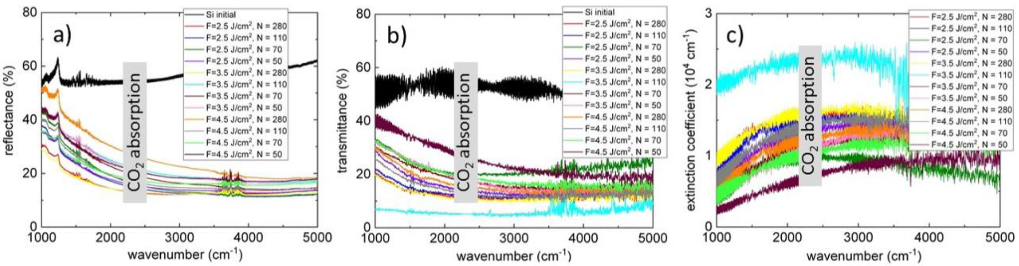
For comparison, FT-IR spectroscopy is related to multi-micrometer penetration depths in Si [52], being rather insensitive to its sub-micrometer thick surface modifications, e.g., optically-thin surface layers of amorphous a-, α- or β-Si3N4 phases (absorption range of 700-1100 cm-1 [24,48,56]). Specifically, in our study the microtextured/doped Si surfaces exhibit considerable broadband (2-10 μm) light scattering/trapping, becoming evident both in the strongly reduced IR reflectance and transmittance acquired in air (Figure 9). The high-wavenumber increase of extinction coefficient indicates that long-wavelength absorption of free carriers, which could emerge due to thermal ionization of the predominating donor nitrogen centers and are present inside gold nanoparticles, appears negligible (see also our electro-physical characterization data below). Basically, Au- and, mostly, N-dopant IR absorption occurs in nitrogen pair (Ni-Ni) centers at 770 and 960 cm-1 [53], off-center substitutional nitrogen Ns (550, 770 and 890 cm-1 [53], aggregates with vacancies (V) and Si self-interstitials (I) – (Ns-Ns), (Ni-Ni)V, (N)2I etc. [32], being enhanced by scattering/trapping. Importantly, the spectral variations of reflectance, transmittance and extinction coefficient are lower at the maximal fluence F = 4.5 J/cm2, supporting the observation of stronger ablative plasma screening on the Si surface under this fluence and corresponding exposures.
Finally, we performed room-temperature van der Paw and Hall measurements of electrical characteristics of the laser-modified Si surface layer. These measurements exhibit the high carrier mobility of 1050 cm2/Vs and carrier sheet concentration ~2×1010 cm-2 (bulk concentration ~1014-1015 cm-3), which are reasonably consistent with the corresponding room-temperature parameters in nitrogen-implanted/annealed Si samples ((3-4)×102 cm2/Vs and ~1017 cm-3) [40]. The high carrier mobility implies the good crystalline quality of the layer, while the rather low carrier concentration indicates negligible dopant segregation effects and low thermal ionization of the deep donor states of nitrogen (0.2-0.3 eV [40]) and donor/acceptor states of gold (Au donor/acceptor centers) in Si.
4. Conclusions
Novel double-impurity doping process for Si surfaces was explored, proceeding via nanosecond-laser co-melting of a top Au film and a Si wafer substrate in a laser plasma-activated LN environment. The fluence- and exposure-independent surface micro-spike topography contains minor Au (~0.1 at. %) and major N (~10 at. %) dopants, localized in a sub-100-nm thick surface layer. X-ray photoelectron spectroscopy indicated bound surface (SiNx) and bulk doping nitrogen states, with the nitrogen and oxygen dopant bulk distributions strongly reduced by the competing gold dopant with its two orders of magnitude lower concentrations. The slight reduction of the crystalline order was revealed by in the second-order Si phonon band, along with nanoscale dimensions of the resolidified Si nano-crystallites, negligible a-Si abundance and Si3N4 surface coating layer. IR 2D-mapping exhibited the only broad structureless absorption bands in the range of 1000-5000 cm-1 related to dopant absorption and light-trapping in the surface micro-relief. The room-temperature electrical characteristics of the laser-nitrified Si layer – carrier mobility of ~1×103 cm2/Vs and background carrier sheet concentration ~1014-1015 cm-3 – indicated almost defect-free structure of the doped layer without abundant thermally-ionized shallow impurity centers and Au-segregated nanoparticles, being superior regarding previously reported characteristics of nitrogen-implanted/annealed Si samples. This novel facile double-element laser-doping procedure paves the way toward local maskless on-demand introduction of multiple intra-gap intermediate donor and acceptor bands in Si, providing its related broadband IR photoconductivity for optoelectronic applications.
Author Contributions
Conceptualization, S.K. and V.S..; methodology, S.K., M.K..; formal analysis, M.K., A.N., I.P.; investigation, A.N., N.S., E.U.; writing—original draft preparation, S.K.; writing—review and editing, V.S.; visualization, E.U and V.P.; supervision, S.K.; All authors have read and agreed to the published version of the manuscript.
Funding
These results were obtained in the framework of the State task № FSFN-2024-0019.
Conflicts of Interest
The authors declare no conflicts of interest.
References
- Huang, C.; FuJ.isawa, S.; de Lima, T.F.; et al. A silicon photonic–electronic neural network for fibre nonlinearity compensation. Nat. Electron. 2021, 4, 837-844. [CrossRef]
- Xiang, C.; J.in, W.; Huang, D.; et al. High-performance silicon photonics using heterogeneous integration. IEEE J. SEL TOP QUANT 2021, 28, 1-15. [CrossRef]
- Carroll, L.; Lee, J. S.; Scarcella, C.; et al. Photonic packaging: transforming silicon photonic integrated circuits into photonic devices. Appl. Sci. 2016, 6, 426. [CrossRef]
- Tong, Z.; Bu, M.; Zhang, Y.; Yang, D.; Pi X. Hyperdoped silicon: Processing, properties, and devices. J. Semicond. 2022, 43, 093101. [CrossRef]
- Recht, D.; Smith, M.J..; Charnvanichborikarn, S.; et al. Supersaturating silicon with transition metals by ion implantation and pulsed laser melting. J. Appl. Phys. 2013, 114, 124903. [CrossRef]
- Lim, S.Q.; Williams, J..S. Electrical and Optical Doping of Silicon by Pulsed-Laser Melting, Micro. 2021, 2, 1–22. [CrossRef]
- Fu, J..; Yang, D.; Yu X. Hyperdoped crystalline silicon for infrared photodetectors by pulsed laser melting: A review. Phys. Status Solidi. 2022, 219, 2100772. [CrossRef]
- Kudryashov, S. I.; Nguyen, L. V.; Kirilenko, D. A.; et al. Large-scale laser fabrication of antifouling silicon-surface nanosheet arrays via nanoplasmonic ablative self-organization in liquid CS2 tracked by a sulfur dopant. ACS Appl. Nano Mater. 2018, 1, 2461-2468. [CrossRef]
- Kudryashov, S.; Nastulyavichus, A.; Kirilenko, D.; et al. Mid-Ir-sensitive n/p-J.unction fabricated on p-type Si surface via ultrashort pulse laser n-type hyperdoping and high-temperature annealing. ACS Appl. Electron. Mater. 2021, 3(2), 769-777. [CrossRef]
- Shimabayashi, M.; Kaneko, T.; Sasaki, K. Nitriding of 4H-SiC by irradiation of fourth harmonics of Nd: YAG laser pulses in liquid nitrogen. SN Appl. Sci. 2020, 2, 1-7. [CrossRef]
- Sher, M.-J..; Hemme, E.G. Hyperdoped silicon materials: from basic materials properties to sub-bandgap infrared photodetectors. Semicond. Sci. Technol. 2023, 38, 033001. [CrossRef]
- Ferdous, N.; Ertekin, E. Atomic scale origins of sub-band gap optical absorption in goldhyperdoped silicon, AIP Adv. 2018, 8, 055014. [CrossRef]
- Kudryashov, S.; Boldyrev, K.; Nastulyavichus, A.; et al. Near-far IR photoconductivity damping in hyperdoped Si at low temperatures. Optical Materials Express 2021, 11, 3792-3800. [CrossRef]
- Sher, M.-J..; Mazur, E. Intermediate band conduction in femtosecond-laser hyperdoped silicon, Appl. Phys. Lett. 2014, 105, 032103. [CrossRef]
- Shao, H.; Liang, C.; Zhu, Z.; et al. Hybrid functional studies on impurity-concentration-controlled band engineering of chalcogen-hyperdoped silicon. Appl. Phys. Express 2013, 6, 085801. [CrossRef]
- Ertekin, E.; Winkler, M. T.; Recht, D.; et al. Insulator-to-metal transition in selenium-hyperdoped silicon: observation and origin. Phys. Rev. Lett. 2012, 108, 026401. [CrossRef]
- Vavilov, V.S.; Chelyadinskii, A.R. Impurity ion implantation into silicon single crystals: efficiency and radiation damage. Phys. Usp. 1995, 38, 333–343. [CrossRef]
- Dissanayake, S.S.; Pallat, N.O.; Chow, P.K.; et al. Carrier lifetimes in gold–hyperdoped silicon—Influence of dopant incorporation methods and concentration profiles. APL Mater. 2022, 10, 111106. [CrossRef]
- Sher, M.J..; Simmons, C.B.; Krich, J..J..; et al. Picosecond carrier recombination dynamics in chalcogen-hyperdoped silicon. Appl. Phys. Lett. 2014, 105, 053905. [CrossRef]
- Newman, B. K.; Sher, M. J..; Mazur, E.; Buonassisi, T. Reactivation of sub-bandgap absorption in chalcogen-hyperdoped silicon. Appl. Phys. Lett. 2011, 98, 251905. [CrossRef]
- Kudryashov, S.; Nastulyavichus, A.; Krasin, G.; et al. CMOS-compatible direct laser writing of sulfur-ultrahyperdoped silicon: Breakthrough pre-requisite for UV-THz optoelectronic nano/microintegration. Opt. Laser Technol. 2023, 158, 108873. [CrossRef]
- Iori, F.; Degoli, E.; Palummo, M.; Ossicini, S. Novel optoelectronic properties of simultaneously n-and p-doped silicon nanostructures. Superlattice Microst. 2008, 44, 337-347. [CrossRef]
- Wang, L.Y.; Zhou, R.H.; Liu, Y.F.; et al. Simulation and typical application of multi-step diffusion method for MEMS device layers. Key Eng. Mat. 2015, 645, 341-346. [CrossRef]
- Kudryashov, S.I.; Nastulyavichus, A.A.; Pryakhina, V.I.; et al. Nanosecond-laser nitridation and nitrogen doping of silicon wafer surface in liquid nitrogen. Ceram. Int. 2024, submitted. [CrossRef]
- Yang, D.; Ma, X.; Fan, R.; et al. Oxygen precipitation in nitrogen-doped Czochralski silicon. Physica B: Condensed Matter. 1999, 273, 308-311. [CrossRef]
- Akatsuka, M.; Sueoka, K. Pinning effect of punched-out dislocations in carbon-, nitrogen-or boron-doped silicon wafers. J.PN J. Appl. Phys. 2001, 40, 1240. [CrossRef]
- Yang, D.; Chu, J..; Xu, J..; Que D. Behavior of oxidation-induced stacking faults in annealed Czochralski silicon doped by nitrogen. J. Appl. Phys. 2003, 93, 8926-8929. [CrossRef]
- Ammon, W.; Ho¨lzl, R.; Virbulis, J..; et al. The impact of nitrogen on the defect aggregation in silicon. J. Cryst. Growth. 2001, 226, 19-30. [CrossRef]
- Yu, X. Yang, D.; Hoshikawa K. Investigation of nitrogen behaviors during Czochralski silicon crystal growth. J. Cryst. Growth 2011, 318, 178-182. [CrossRef]
- Masuda, A.; Itoh, K.I.; Matsuda, K.; et al. Y. Nitrogen-doping effects on electrical, optical, and structural properties in hydrogenated amorphous silicon. J. Appl. Phys. 1997, 81, 6729-6737. [CrossRef]
- Sgourou, E. N.; Angeletos, T.; Chroneos, A.; Londos, C.A. Infrared study of defects in nitrogen-doped electron irradiated silicon. J. Mater. Sci. Mater. Electron. 2016, 27, 2054–2061. [CrossRef]
- Platonenko, A.; Gentile, F.S.; Pascale, F.; et al. Nitrogen substitutional defects in silicon. A quantum mechanical investigation of the structural, electronic and vibrational properties. Phys. Chem. Chem. Phys. 2019, 21, 20939–20950. [CrossRef]
- Wang, W.; Ma, S.X.; Liu, X.; et al. NO2 gas sensor with excellent performance based on thermally modified nitrogen-hyperdoped silicon. Sensors Actuators B: Chem. 2022, 354, 131193. [CrossRef]
- Potsidi, M.S.; Kuganathan, N.; Christopoulos, S.-R. G.; et al. Theoretical investigation of nitrogen-vacancy defects in silicon. AIP Adv. 2022, 12, 025112. [CrossRef]
- Yatsurugi, Y.; Akiyama, N.; Endo, Y.; Nozaki, T. Concentration, solubility, and equilibrium distribution coefficient of nitrogen and oxygen in semiconductor silicon. J. Electrochem. Soc. 1973, 120, 975-979. [CrossRef]
- Belli, M.; Fanciulli, M. Electron Spin–Lattice Relaxation of Substitutional Nitrogen in Silicon: The Role of Disorder and Motional Effects. Nanomaterials 2023, 14, 21. [CrossRef]
- Murakami, K.; Itoh, H.; Takita, K.; Masuda, K. Substitutional nitrogen impurities in pulsed-laser annealed silicon. Appl. Phys. Lett. 1984, 45, 176–178. [CrossRef]
- J.ones, R.; Hahn, I.; Goss, J..P.; et al. Structure and Electronic Properties of Nitrogen Defects in Silicon. Solid State Phenom. 2003, 95-96, 93–98. [CrossRef]
- Dong, X.; Li, N.; Zhu Z. A nitrogen-hyperdoped silicon material formed by femtosecond laser irradiation. Appl. Phys. Lett. 2014, 104, 091907. [CrossRef]
- Stein, H.J. Nitrogen in Crystalline Si. MRS Online Proceedings Library 1985, 59, 523–535. [CrossRef]
- Stein, H.J. Nitrogen related donors in silicon. J. Electrochem. Soc. 1987, 134, 2592. [CrossRef]
- Kobayashi, S.I. IR spectroscopic study of silicon nitride films grown at a low substrate temperature using very high frequency plasma-enhanced chemical vapor deposition. World J. Condensed Matter Phys. 2016, 6, 287-293. [CrossRef]
- Mihailescu, I.N.; Litã, A.; Teodorescu, V.S.; et al. Synthesis and deposition of silicon nitride films by laser reactive ablation of silicon in low pressure ammonia: A parametric study. J. Vac. Sci. Technol. A 1996, 14, 1986-1994. [CrossRef]
- Blumenthal, D. J..; Heideman, R.; Geuzebroek, D.; et al. Silicon nitride in silicon photonics. Proceedings of the IEEE 2018, 106, 2209-2231. [CrossRef]
- Barkby, J..; Moro, F.; Perego, M.; et al. Fabrication of nitrogen-hyperdoped silicon by high-pressure gas immersion excimer laser doping. Sci. Rep. 2024, 14, 19640. [CrossRef]
- Kanaya, K.; Okayama, S. Penetration and energy-loss theory of electrons in solid targets. J. Phys. D. Appl. Phys. 1972, 5, 43. [CrossRef]
- Kudryashov, S.I.; Allen, S.D. Photoacoustic study of KrF laser heating of Si: Implications for laser particle removal. J. Appl. Phys. 2002, 92, 5627-5631. [CrossRef]
- Wada, N.; Solin, S.A.; Wong, J..; Prochazka, S. Raman and IR absorption spectroscopic studies on α, β, and amorphous Si3N4. J. of Non-Cryst. Solids 1981; 43, 7-15. [CrossRef]
- NIST X-ray Photoelectron Spectroscopy Database. Available online: https://srdata.nist.gov/xps/ElmComposition (accessed 15 J.une 2024).
- Ermolieff, A.; Bernard, P.; Marthon, S.; Camargo da Costa, J. Nitridation of Si (100) made by radio frequency plasma as studied by in situ angular resolved x-ray photoelectron spectroscopy. J. Appl. Phys. 1986, 60, 3162–3166. [CrossRef]
- Peters, S.; Peredkov, S.; Neeb, M.; et al. Size-dependent XPS spectra of small supported Au-clusters. Surf. Sci. 2013, 608, 129–134. [CrossRef]
- Palik, E.D. Handbook of optical constants of solids, 3rd ed.; Academic press: San Diego, USA, 1998; p. 1000.
- Goss, J. P.; Hahn, I.; J.ones, R.; et al. Vibrational modes and electronic properties of nitrogen defects in silicon. Phys. Rev. B 2003, 67, 045206. [CrossRef]
- Viera G., Huet, S.; Boufendi, L. Crystal size and temperature measurements in nanostructured silicon using Raman spectroscopy. J. Appl. Phys. 2001, 90, 4175-4183. [CrossRef]
- Ehara, T. Electron spin resonance study of nitrogen-doped microcrystalline silicon and amorphous silicon. Appl. Surf. Sci. 1997, 113, 126-129. [CrossRef]
- Luongo, J.P. IR study of amorphous silicon nitride films. Appl. Spectrosc. 1984, 38, 195-199. [CrossRef]
Figure 1.
Experimental layout: 532-nm 10-ns Nd:YAG laser, focusing cylindrical lens, thermally-isolating reaction cell with the Si wafer immersed into LN, 2D micro-positioning stage.
Figure 1.
Experimental layout: 532-nm 10-ns Nd:YAG laser, focusing cylindrical lens, thermally-isolating reaction cell with the Si wafer immersed into LN, 2D micro-positioning stage.
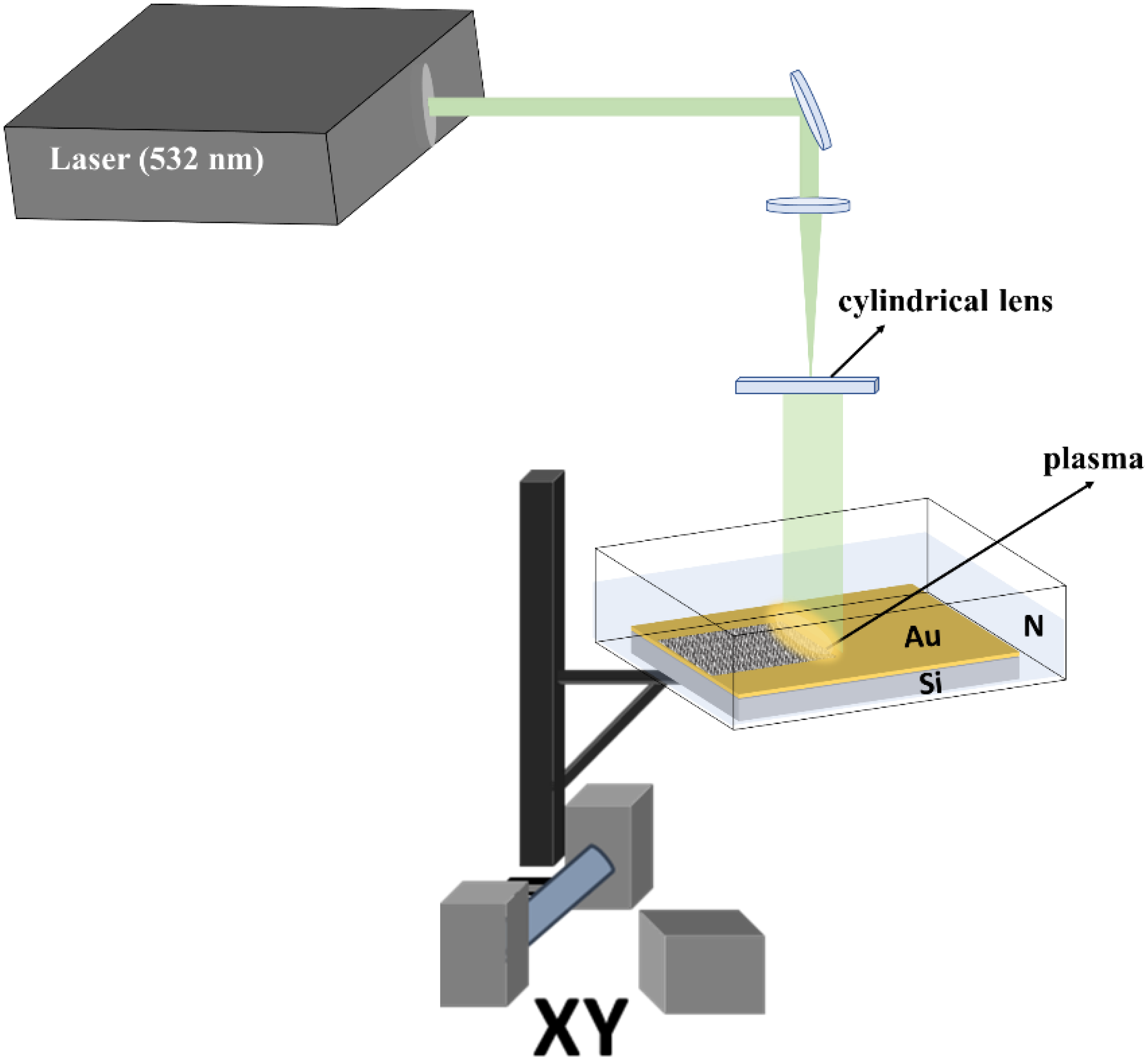
Figure 2.
SEM images of Si wafer topography laser-textured at different fluences F=2.5-4.5 J/cm2 and exposures N =50-280.
Figure 2.
SEM images of Si wafer topography laser-textured at different fluences F=2.5-4.5 J/cm2 and exposures N =50-280.
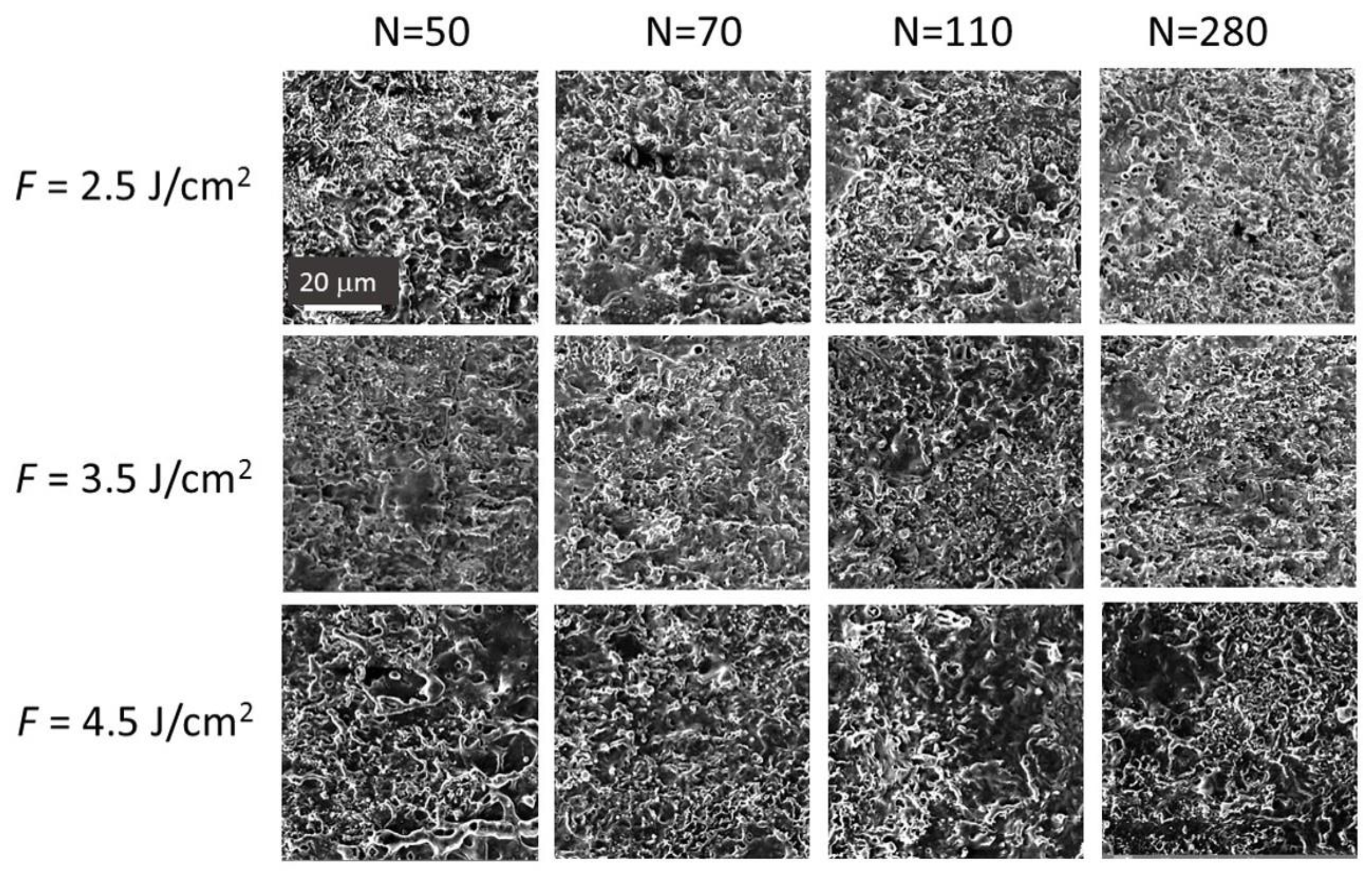
Figure 3.
a) Combined and separate EDX elemental maps for gold, oxygen, nitrogen and silicon at 5-kV voltage and laser parameters of 3.5-J/cm2 fluence and 280-pulse exposure. Dependences of gold (b) and nitrogen (c) atomic content (%) probed at the 5-kV voltage, versus laser fluence at different exposures of 50, 70, 110 and 280 pulses/spot. Additionally, 150-cm-1 Raman peak intensity for Si3N4 is shown in (c) for comparison.
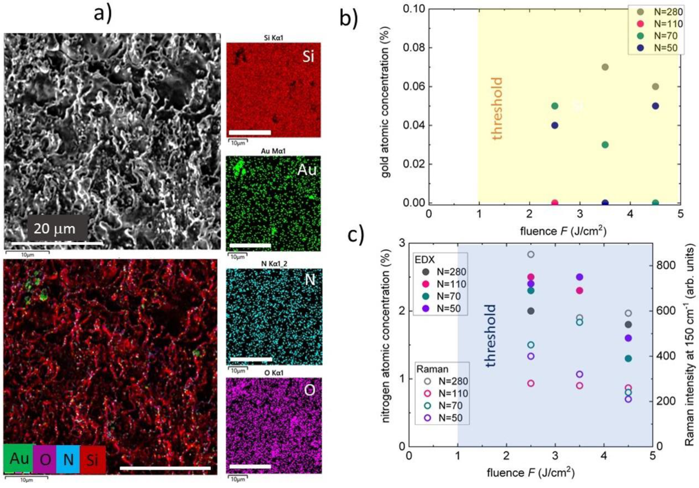
Figure 4.
XPS binding energy spectra for Si (a), N (b), Au (c), O (d), and C (e) elements with their spectral decomposition and assignment after [49]. (f) Fluence dependence of elemental atomic content for N (dark symbols) and Au (light symbols) at different laser exposures N =50-280 pulses/spot.
Figure 4.
XPS binding energy spectra for Si (a), N (b), Au (c), O (d), and C (e) elements with their spectral decomposition and assignment after [49]. (f) Fluence dependence of elemental atomic content for N (dark symbols) and Au (light symbols) at different laser exposures N =50-280 pulses/spot.
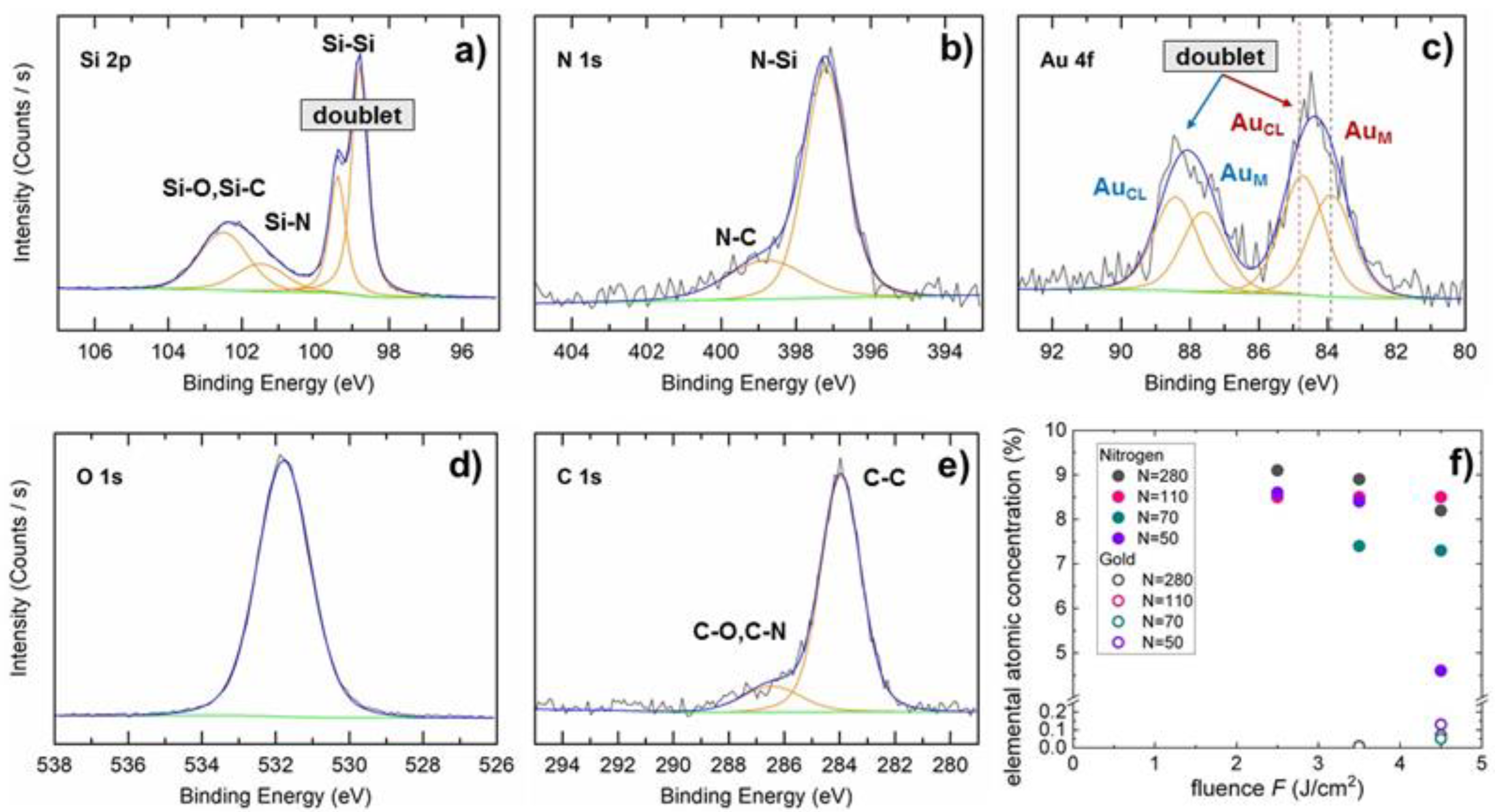
Figure 5.
Depth-dependent XPS binding energy spectra for Si (a), O (b), N (c) and Au (d) elements with their spectral assignment after [49], acquired at the Si spot modified at F = 2.5 J/cm2 and N = 50 pulses/spot.
Figure 5.
Depth-dependent XPS binding energy spectra for Si (a), O (b), N (c) and Au (d) elements with their spectral assignment after [49], acquired at the Si spot modified at F = 2.5 J/cm2 and N = 50 pulses/spot.
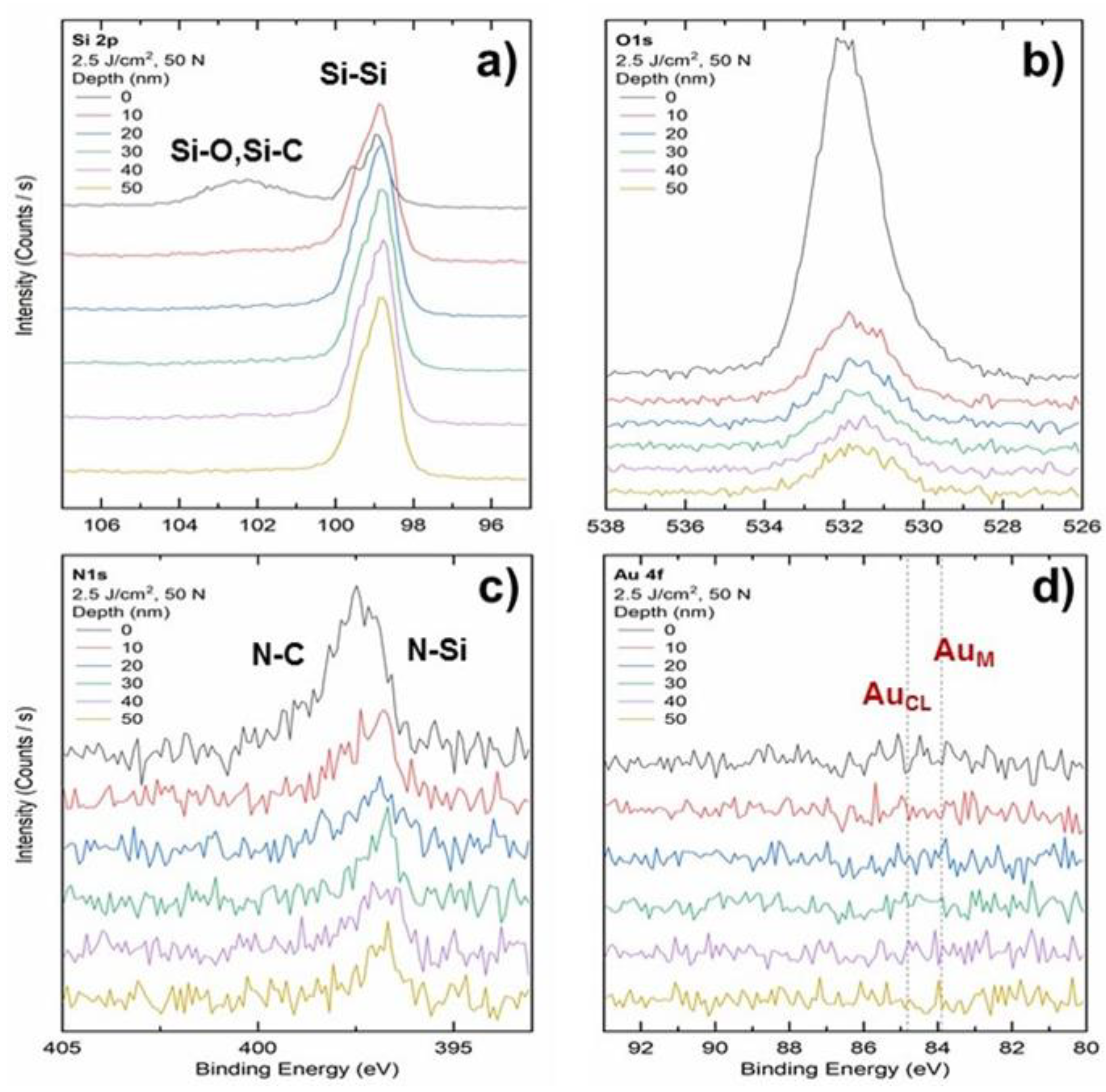
Figure 6.
Depth-dependent XPS binding energy spectra for Si (a), O (b), N (c) and Au (d) elements with their spectral assignment after [49], acquired at the Si spot modified at F = 4.5 J/cm2 and N = 50 pulses/spot.
Figure 6.
Depth-dependent XPS binding energy spectra for Si (a), O (b), N (c) and Au (d) elements with their spectral assignment after [49], acquired at the Si spot modified at F = 4.5 J/cm2 and N = 50 pulses/spot.
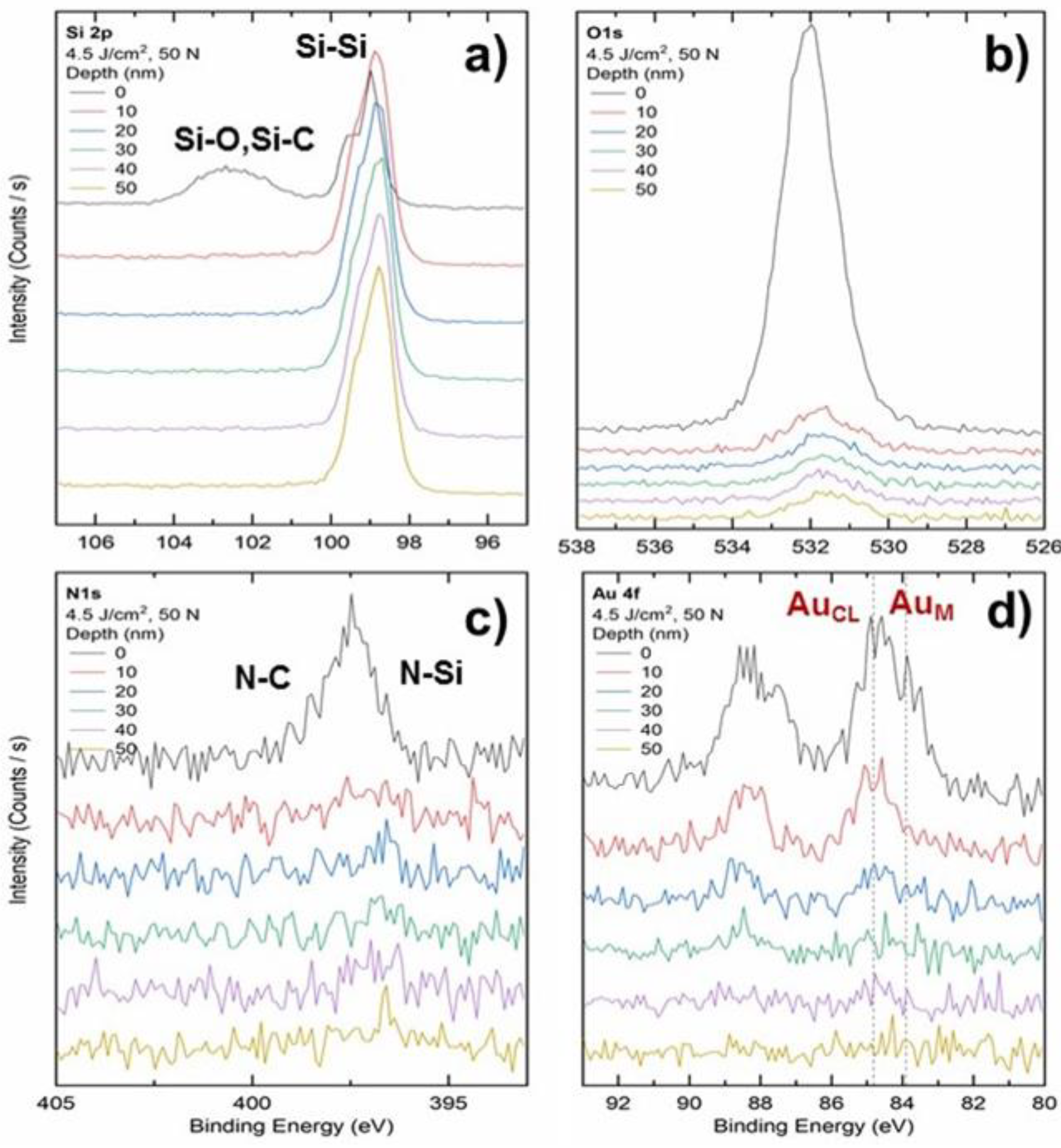
Figure 7.
XPS-acquired depth-dependent abundance of nitrogen and gold at laser fluence F = 2.5, 3.5 and 4.5 J/cm2 for N =50 pulses/spot. The total gold content acquired for the Au4f7/2 line at F = 4.5 J/cm2 for N =50 pulses/spot, is distinguished between the metallic (AuM) and cluster (AuCL) components.
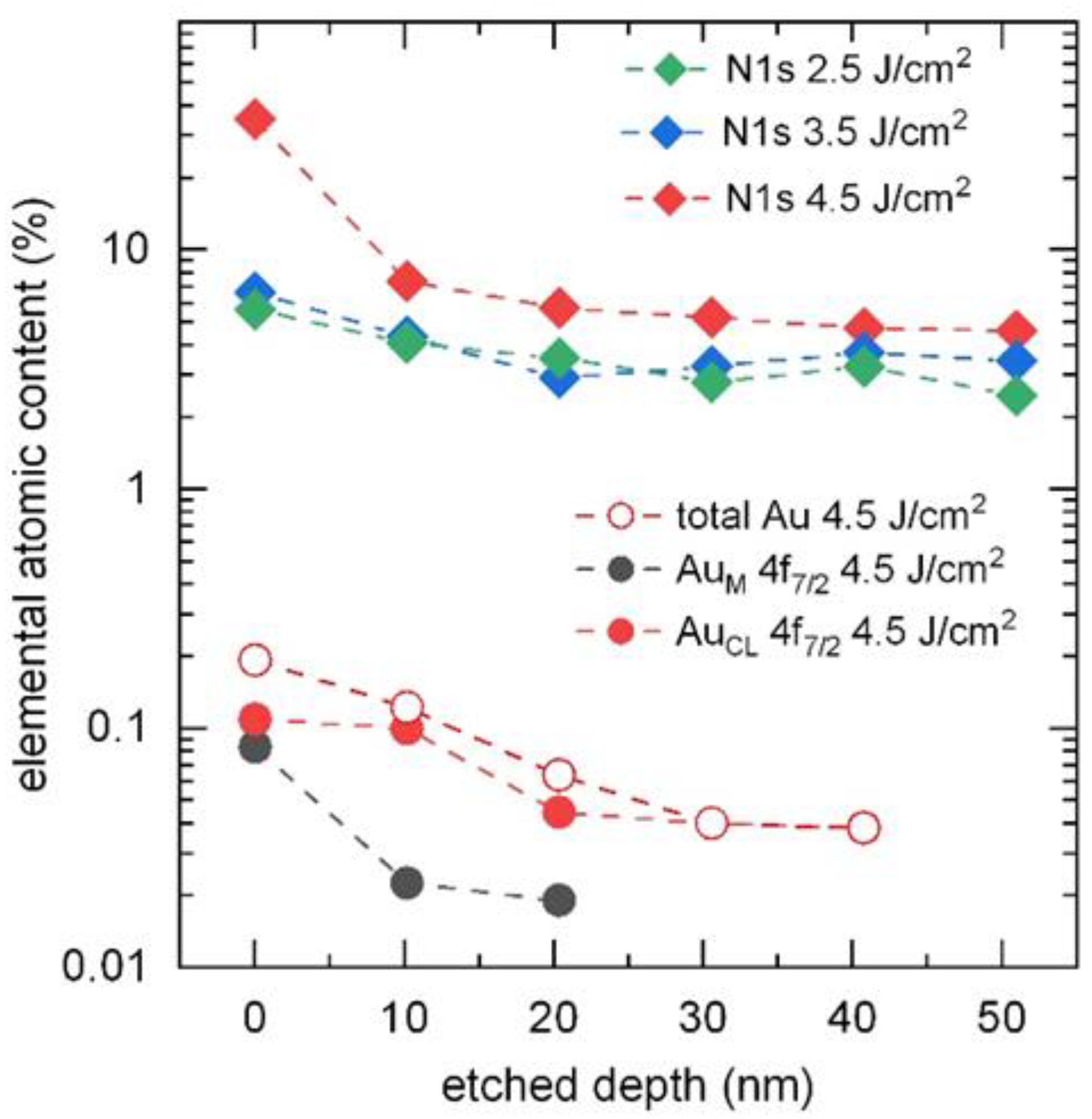
Figure 8.
Raman spectra of the laser-doped samples, prepared at different fluence and exposure values, at 532-nm pumping (reference sample – c-Si): (a) panoramic view; (b) main 521-cm-1 LO/TO Raman peak fitted by Lorentzian curves (inset – Si crystallite dimensions derived from the FWHM values of the peak, versus laser fluence); (с) second-order Si band; (d) low-wavenumber Si3N4-band. Spectral assignments after [32,48,53].
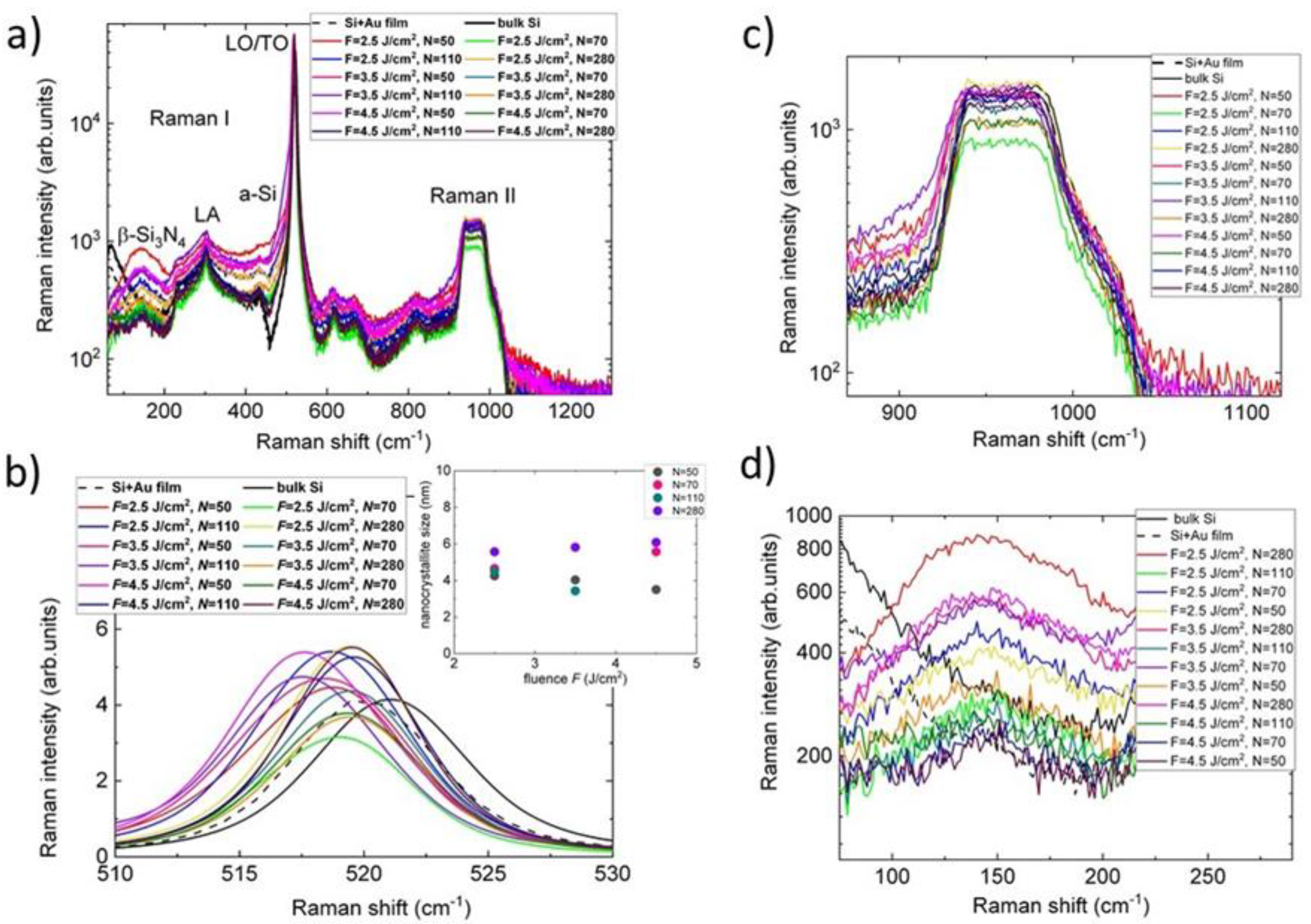
Figure 9.
FT-IR reflectance (a), transmittance (b) and extinction coefficient (c) spectra of laser-modified/doped samples prepared at different fluence and exposure values (reference sample – c-Si).
Figure 9.
FT-IR reflectance (a), transmittance (b) and extinction coefficient (c) spectra of laser-modified/doped samples prepared at different fluence and exposure values (reference sample – c-Si).
Disclaimer/Publisher’s Note: The statements, opinions and data contained in all publications are solely those of the individual author(s) and contributor(s) and not of MDPI and/or the editor(s). MDPI and/or the editor(s) disclaim responsibility for any injury to people or property resulting from any ideas, methods, instructions or products referred to in the content. |
© 2024 by the authors. Licensee MDPI, Basel, Switzerland. This article is an open access article distributed under the terms and conditions of the Creative Commons Attribution (CC BY) license (http://creativecommons.org/licenses/by/4.0/).
Copyright: This open access article is published under a Creative Commons CC BY 4.0 license, which permit the free download, distribution, and reuse, provided that the author and preprint are cited in any reuse.


