Submitted:
07 December 2025
Posted:
08 December 2025
You are already at the latest version
Abstract
This project aims to develop a basic predictive maintenance model for aviation sensors, especially the ones that are directly related to flight safety. The study first uses SCAPS-1D to simulate a simple semiconductor structure and observe how electrical parameters such as Voc and Jsc change with temperature and material conditions. After getting these results, a simple state-space model is built in MATLAB to represent the relation between temperature input and device output. The idea is that many aircraft sensors, like the Angle of Attack (AOA) sensor, also contain small pn junction electronics inside, and their failures often begin with small drifts in electrical behavior. By comparing the SCAPS results with the state-space model, the project shows how these changes can be used as early indicators of degradation. This work gives a starting framework for future predictive maintenance studies by connecting semiconductor modeling with aviation sensor health monitoring.
Keywords:
Solid state electronics
; sensors
; failure
; system response
I. Introduction
Aviation technology is improving day by day, and the most important thing in aviation is safety. Because of this, all aviation authorities try to build safer systems and install the newest technologies on aircraft. Maintenance is also one of the most important responsibilities for aviation companies, and only certified places that have EASA Part-66 and Part-145 authorization can perform it.
Even though maintenance companies spend a lot of money on their staff, follow strict procedures, and take many precautions before releasing an aircraft back to service, we still sometimes face critical system problems.
The aim of this study is to examine a specific type of aviation sensor and look inside how it works on a solid-state level. The study will compare different structures and comment on which one could be more useful or more reliable to prevent
II. Litereatıre Review
Some studies examine the general working principle of solar cell structure. In reference [1] they explain the basic solar cell structure and device characteristics, starting from morphology, I-V, PCE and QE parameters. They choose Antimony Triselenide (Sb₂Se₃) because it gives optimum band gap alignment and also non-toxic option for solar cell applications.
Another study in reference [2] looked detailed parameters of solar cell structure by using SCAPS software. SCAPS provides optical information of 1D and 2D materials. In that study they compared BaZrSe₃ and CsPbI₃ for photovoltaic applications.
Another important source for my study is NASA Aviation Safety Report System (ASRS). NASA shares critical events and failures in aviation such as sensor faults, system malfunctions, electronics problems etc. Many aviation sensors actually work with same physics of a solar cell (pn junction). For example: angle of attack sensors, ice and rain protection system sensors, brake temperature monitoring sensors, cargo fire/overheat warning sensors, smoke detectors, and some navigation systems. Some of them are directly related with photo-diode mechanism and some others are indirectly using pn-junction for temperature compensation or signal stabilization.
For my scope the most relevant sensor is Angle of Attack (AOA) sensor.
III. Problem Definition
The aim of this study is to create an extra check method for one of the most problematic systems which is used in aviation and its working mechanism is connected to photo-diode / solar-cell physics. The selected sensor for my application is Angle of Attack (AOA) sensor.
Most aircraft (Boeing, Airbus, Embraer, CRJ, Cessna) use vane-type AOA sensors. AOA has two main parts: one mechanical and one electronics.
Mechanical Part
The mechanical part has two basic duties.
- First, a small aerodynamic vane rotates freely and aligns itself to the local airflow.
- Second, the rotation angle of this vane becomes equal to angle between airflow and wing chord. So if aircraft pitch changes, the vane follows that airflow change.
- This gives a mechanical rotation directly proportional to Angle of Attack.
Electronics Part
Inside the AOA sensor housing there are electronics which change this rotation into an electrical signal. There are mainly three technologies used:
- (A) Resolver / Synchro Type
- The vane shaft connects to a rotor.
- The rotor is inside stator coils.
- AC excitation is applied.
- As the rotor turns, induced voltages (sinθ, cosθ) change.
- The ECU converts these voltages into AOA value.
This is the most common on big jets.
- (B) Hall-Effect Sensor Type
Modern AOA sensors use magnets attached to the vane shaft, and a Hall-effect IC measures the magnetic angle.
- Output can be 0-5V or ARINC-429 digital.
- This system also needs internal temperature compensation.
- (C) Potentiometer Type
Used in older or small aircraft.
- The vane rotates a wiper over a resistive track and output voltage changes with angle.
- Cheap but more drift and wear problems.
Temperature Compensation Need
AOA sensors sit outside the aircraft, so they see freezing cold, hot air, rain, vibration, ice, humidity. Electronics inside can suffer:
- resistance drift
- diode drift
- offset voltage changes
- leakage currents
So all modern AOA sensors include a PN-junction temperature compensation diode.
- When this diode degrades:
- Rs increases because of corrosion → signal drop
- Rsh decreases because of moisture → noisy or fluctuating angle
- Nt increases → diode equation shifts → calibration drift
- AOA becomes unreliable (stick shaker activation, unreliable airspeed etc.)
NASA ASRS reports show these exact types of failures many times.
Purpose of Simulation
In this study the purpose is the simulation of PN-junction structure responses according to some parameters and see the possible output behavior of the AOA sensor. SCAPS software will be used to simulate how changes in Rs, Rsh, defect density (Nt) and temperature can influence the sensor output.
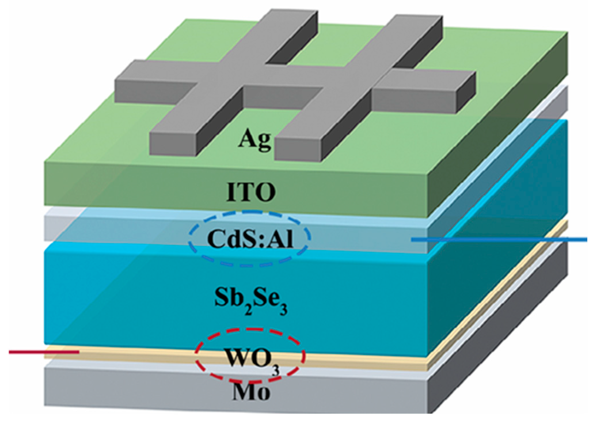
Before that, a simple solar cell structure will be examined (Figure 1) to understand the core mechanism which later also appears in AOA sensor electronics.
In this figure I look at a very simple solar cell structure just to understand how the layers sit on each other and what each one is doing. Because later, the same pn-junction idea and some of this layer logic also appears inside the AOA sensor electronics (especially the temperature-compensation diode). So this small explanation helps me see the whole mechanism more clearly.
The example structure has six layers. At the very top there is Ag (Silver) metal contact. This layer collects the electrons which are generated inside the absorber and it also works like the top electrode of the device. Under the silver layer there is ITO (Indium Tin Oxide). ITO is a transparent conductive oxide, which means it lets light go through but it also conducts current. So basically it is the “window” of the device.
After ITO comes the buffer layer, which in this study is CdS:Al. This layer forms the pn-junction with the absorber material, and it also blocks unwanted holes and transmits the electrons. So the buffer layer is like the “separator” and it controls how charges move between layers.
Below that is the main absorber which is Sb₂Se₃. This is the most important layer because light is absorbed here and electron–hole pairs are created. All the performance (PCE, I-V, QE etc.) are mostly depending on this absorber quality.
Under the absorber there is an interface layer, here it is WO₃ (Tungsten Trioxide). This layer improves the back contact, helps hole extraction, and sometimes reduces recombination at the backside. It is like a buried layer that improves electrical performance.
Finally, at the bottom there is the Mo (Molybdenum) contact. This is the bottom electrode, and it makes a good ohmic contact especially to p-type materials. So Mo helps collect the charges that move downward.
Overall this stack creates the basic solar cell mechanism: light enters from the top, generates carriers in the absorber, and the top/bottom contacts collect them. This same pn-junction behaviour is also seen in photodiodes and even in the temperature-compensation diode inside the AOA sensor.
Figure 2.
from [4].
Figure 2.
from [4].
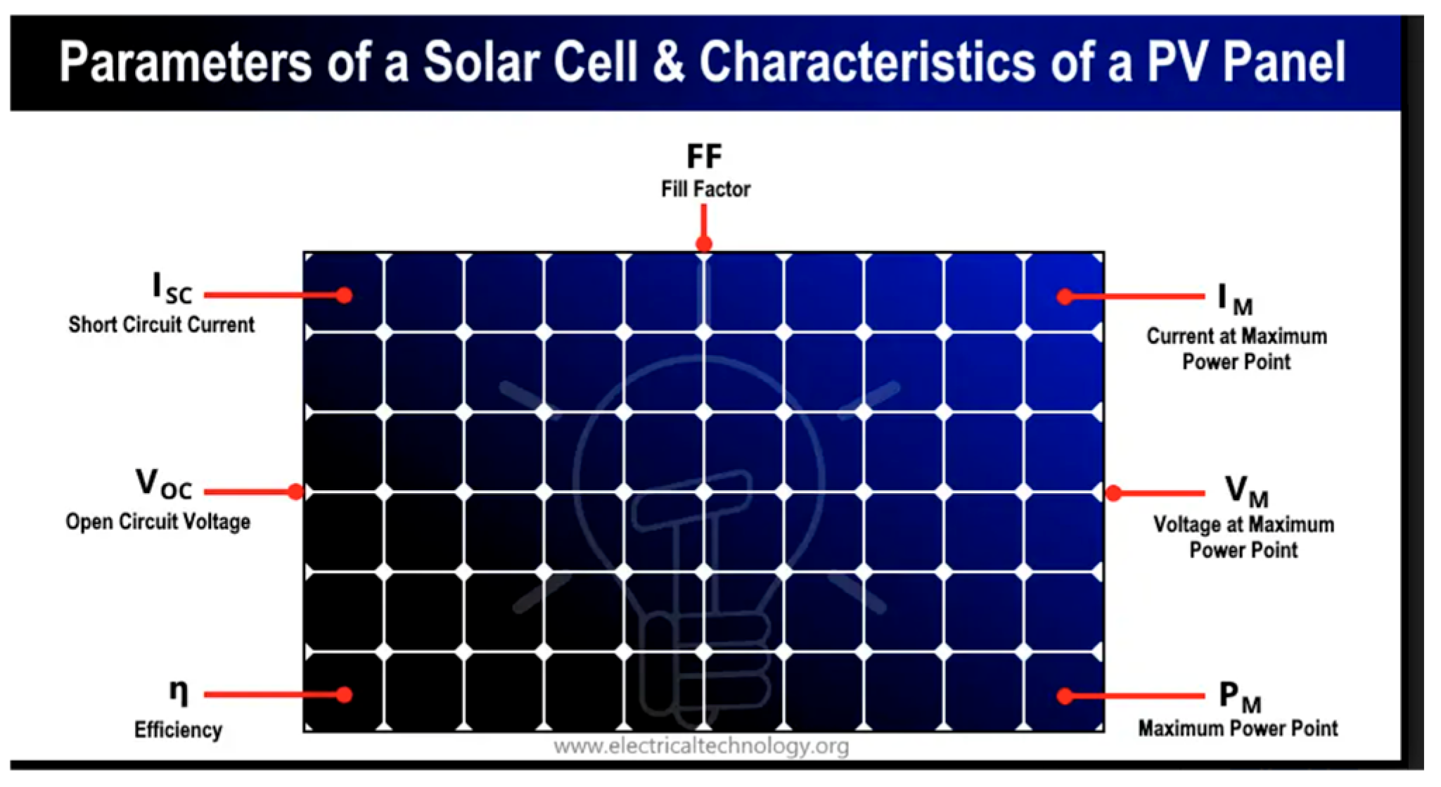
When we look at a solar cell or any PV device, there are some main parameters that basically show how good the device is working. These values come from the I-V curve and they change a lot depends on materials, defects, temperature, junction quality etc. So here I explain the important ones shortly.
1. VOC—Open Circuit Voltage
VOC means the maximum voltage you can get from the device when there is no current flowing (open circuit).It shows how well the band alignment is, and how strong the built-in electric field is inside the pn-junction. If defects increase or the interface is bad, VOC usually goes down. In the table C-device has 0.451 V and Li-device has 0.462 V, so Li doping little bit improve the band alignment.
2. JSC—Short Circuit Current
JSC is the maximum current when the device is shorted (voltage = 0).This value mostly depends on how good the absorber material absorbs light and how well the charge carriers can move without recombining.
3. FF—Fill Factor
FF (fill factor) is kind of the “quality of power extraction”.It depends on series resistance, shunt resistance, contact problems and internal defects.
4. PCE—Power Conversion Efficiency
PCE is the final efficiency of the device.
Relation of PV Parameters and Layer Structure to Angle of Attack Sensor Failures
Even if an Angle of Attack (AOA) sensor is not a real solar cell, inside the sensor there is a small pn-junction diode for temperature compensation and sometimes for signal stabilization. Because of that the basic PV parameters like VOC, ISC, FF and also the idea of absorber layer, contacts and interface layers become important to understand failure behavior. When VOC of the diode starts to drop or change, the AOA output voltage also shifts and this makes wrong angle readings. If ISC increases too much it means leakage current or moisture is entering the device, and this usually creates noisy or jumping AOA values. The fill factor (FF) also reflects the resistive problems, like high series resistance from corrosion or low shunt resistance from contamination, and these problems are reported in NASA ASRS AOA faults. The layer logic of a solar cell (absorber, ETL/HTL, metal contacts) is not exactly same in AOA sensor, but the degradation type is similar. For example bad interface or increased defect density in the junction can make the temperature-compensation diode drift and then AOA calibration goes wrong. So studying these PV parameters in SCAPS helps to understand how the AOA sensor diode changes with aging and why the sensor starts giving unreliable signals.
IV. Mathematical Method
I selected SCAPS software to make simulation of device. I decided my possible best solar structure (Al/FTO/CdS/Se3SbCI3/Au) to simulate angle of attack vane.
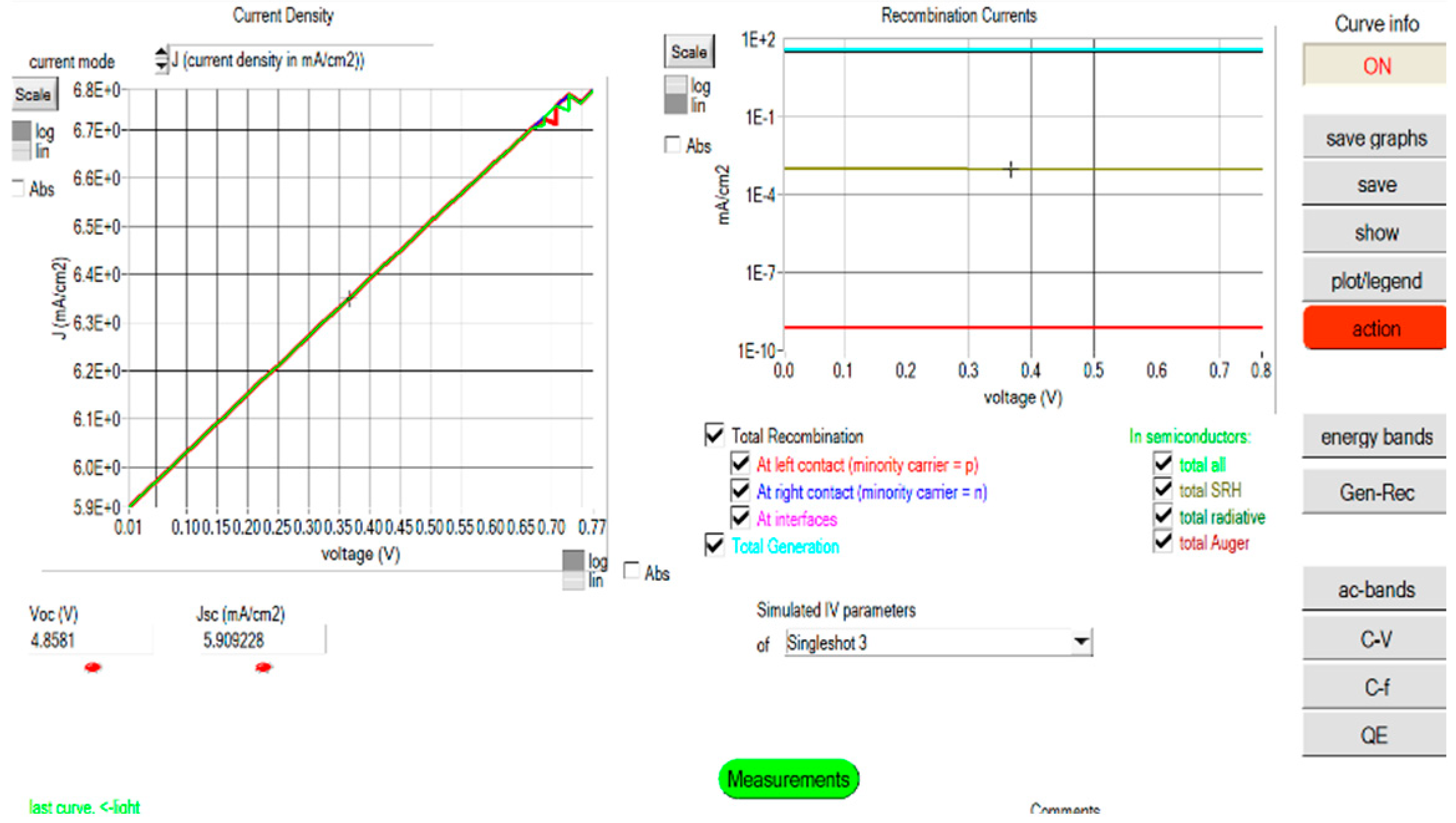
Figure 3.
pn junction in SCAPS software.
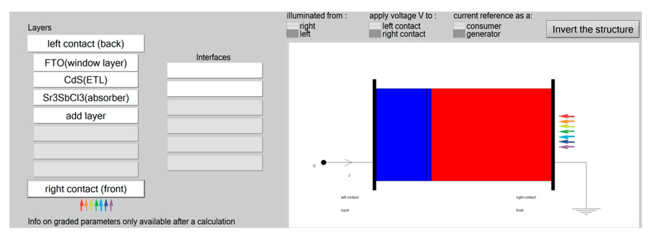
Figure 4.
SCAPS parameter.
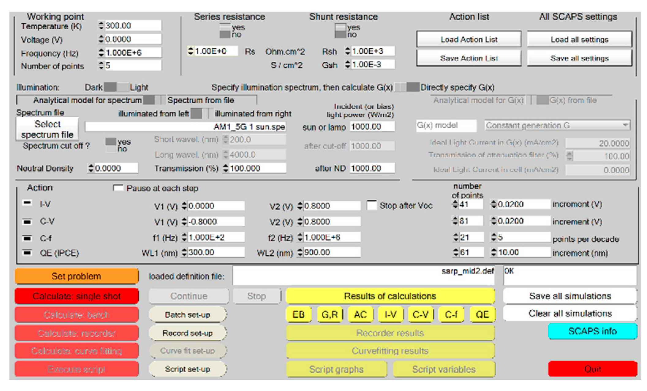
Figure 5.
Device output at 300k Energy diagrams.
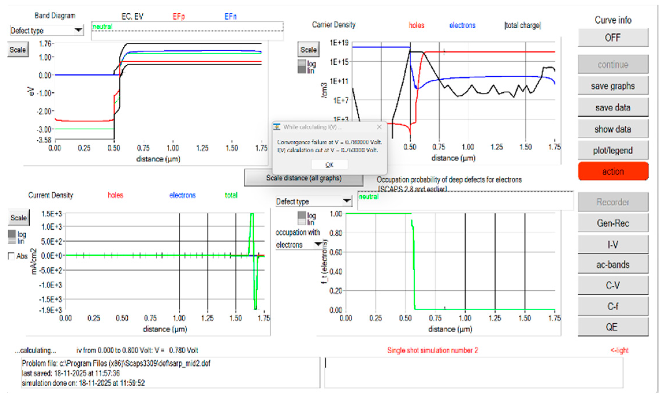
Figure 6.
Device outpus I-V curve.
SCAPS Results and State-Space Analysis
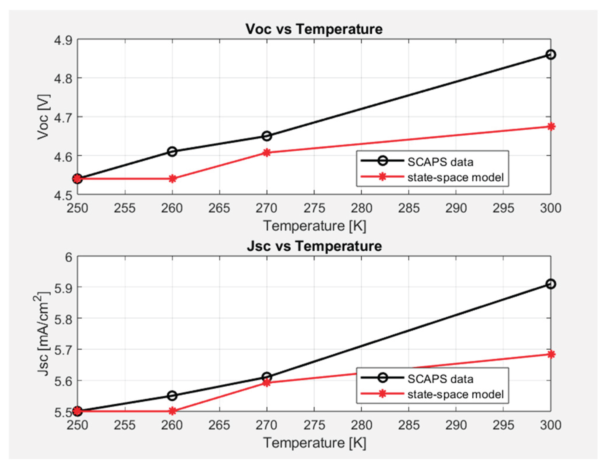
In this study I used SCAPS to simulate my solar-cell structure and see how the device parameters change with temperature. SCAPS gives values like Voc and Jsc at different temperatures. I changed only the temperature (250 K, 260 K, 270 K, 300 K) and observed how the outputs move. These results are the basic input of my mathematical model.
After getting the SCAPS outputs, I used a simple state--space model in MATLAB. The goal was not to build a perfect physical model but to show a basic mathematical relation between temperature change and the change in Voc and Jsc. The state--space system uses x = [Voc; Jsc] and temperature difference as u. The model checks how much the state changes when temperature changes. This is a simple first--order model that a student can build.
The model shows that the device has a small and almost linear sensitivity to temperature. The sensitivity values are inside the B--matrix. This means when temperature increases, Voc and Jsc change a little. The MATLAB plots show that the state--space model follows the SCAPS trend.
This simple method is enough for showing a basic predictive behavior. The idea is that different temperatures cause different sensor outputs. In aviation, angle--of--attack sensors also change their electrical behavior with temperature, aging or internal defects. If the sensor starts giving different drift than expected, it may be an early warning of failure.
In future work I can add more parameters (like Rs, Rsh, defect density) and test a more detailed model. Also real aircraft sensor data can be used to check the model. But for now this basic model is enough to show the principle of using mathematical tools for predictive maintenance.
Figure 7.
Matlab result in State-Space Analysis.
V. Results and Discussion
In this study the SCAPS-1D program was used to simulate a basic multilayer diode structure under different temperatures. SCAPS gives many electrical outputs but in this work we focus mainly on the open-circuit voltage (Voc) and short-circuit current (Jsc). These two parameters change strongly with temperature and also with internal material conditions such as defect density, series resistance and shunt leakage. The SCAPS runs at 250 K, 260 K, 270 K and 300 K show that Voc and Jsc increase slowly when the temperature increases. The band diagrams, carrier density plots and recombination graphs also show that deep level occupation and interface recombination shift with temperature. These SCAPS results prove that small physical changes in the device can be observed from electrical behaviour, which is important for our later fault analysis idea.
To understand this behaviour in a more system-level way, a simple state-space model was created. In the model the state vector contains the main photovoltaic variables (Voc and Jsc) and the input of the system is the temperature change between two operating points. The state-space form allows us to see how the device responds to temperature like a small dynamical system. The model predicts the direction and trend of SCAPS data correctly, and shows how much Voc and Jsc are sensitive to the temperature input. Even if the model is very simple and linear, it still captures the basic device reaction to temperature.
The main motivation is to use this idea for aviation predictive maintenance. Inside an Angle of Attack (AOA) sensor there is also a small pn-junction diode used for temperature compensation and signal stability. When this diode becomes degraded by aging, corrosion or moisture, the output voltage of the AOA sensor starts drifting the same way Voc drifts in a solar diode. Also, when leakage current increases because of contamination, the behaviour is similar to Jsc increase in SCAPS. Because of this, the SCAPS simulations and the state-space model can give a basic understanding how the semiconductor junction inside the AOA sensor will behave under temperature stress and long-term degradation. If the real sensor output moves too far away from the model prediction, this can be a sign of early-stage failure and can be used for maintenance decision.
Future work will include extending the model with more device parameters from SCAPS, such as series resistance, shunt resistance and defect density. These parameters are directly related to common AOA sensor problems like corrosion at connectors or moisture inside the housing. A bigger state-space system or a nonlinear model will be built using more simulation points. Finally, experimental measurements from a real AOA sensor will be compared with the SCAPS-based model to create a practical fault detection or health-monitoring algorithm.
VI. Evaluation and Comparison
In this study the SCAPS simulations and the state-space model were compared to understand the basic relation between temperature and the electrical output of the device. SCAPS gives the real semiconductor behavior, while the state-space model is a simple mathematical representation. Even if the model is very basic, it follows the same trend: when temperature increases, both Voc and Jsc increase slightly. This shows that the model can capture the main device sensitivity with only a few parameters. The comparison also shows that real SCAPS data has more nonlinear behavior, but the linear state-space model is still enough to describe the general direction of change. This evaluation proves that small parameter changes in semiconductor layers can be detected mathematically, which is important when we relate these results to real aviation sensors like the Angle of Attack sensor.
VII. Conclusion and Future Work
The main goal of this project was to understand a simple semiconductor structure with SCAPS and then build a basic mathematical model to show how device parameters change with temperature. The results showed that Voc and Jsc react to temperature in a predictable way and the state-space model can represent this behavior. This idea is useful for predictive maintenance, because the AOA sensor in aircraft also uses a small pn-junction diode inside, and its drift or degradation can be monitored in a similar method. If the real sensor output moves too far away from the expected model, it can be used as an early warning sign of failure. For future work, more parameters such as series resistance, shunt resistance and defect density should be included in the model. Also more SCAPS simulations can be done to build a better and more detailed system representation. Finally, the model needs to be tested with real aircraft sensor data to create a practical health-monitoring or fault-detection method.
References
- Chen, G., Luo, Y., Abbas, M., Ishaq, M., Zheng, Z., Chen, S., Su, Z., Zhang, X., Fan, P., & Liang, G. (n.d.). Suppressing buried interface nonradiative recombination losses toward high-efficiency antimony triselenide solar cells.
- A numerical strategy to achieving efficiency exceeding 27% with a novel dual absorber perovskite solar cell using BaZrSe₃ and CsPbI₃.
- NASA ASRS (n.d.). Aviation Safety Reporting System Database Query Wizard. Available online: https://akama.arc.nasa.gov/ASRSDBOnline/QueryWizard_Filter.aspx.
- Electrical, Technology. Electrical Technology. (2020). Parameters and characteristics of a solar panel explained. Available online: https://www.electricaltechnology.org/2020/09/parameters-characteristics-solar-panel.html.
Figure 1.
from [1] “Simple device structure”.
Figure 1.
from [1] “Simple device structure”.
Disclaimer/Publisher’s Note: The statements, opinions and data contained in all publications are solely those of the individual author(s) and contributor(s) and not of MDPI and/or the editor(s). MDPI and/or the editor(s) disclaim responsibility for any injury to people or property resulting from any ideas, methods, instructions or products referred to in the content. |
© 2025 by the authors. Licensee MDPI, Basel, Switzerland. This article is an open access article distributed under the terms and conditions of the Creative Commons Attribution (CC BY) license (http://creativecommons.org/licenses/by/4.0/).
Copyright: This open access article is published under a Creative Commons CC BY 4.0 license, which permit the free download, distribution, and reuse, provided that the author and preprint are cited in any reuse.


